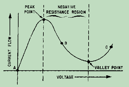
domingo, 30 de mayo de 2010

Varactor Devices


Varactor Devices


The VARACTOR is another of the active two-terminal diodes that operates in the microwave range. Since the basic theory of varactor operation was presented in NEETS, Module 7, Introduction to Solid-State Devices and Power Supplies, Chapter 3, only a brief review of the basic principles is presented here.


The varactor is a semiconductor diode with the properties of a voltage-dependent capacitor. Specifically, it is a variable-capacitance, pn-junction diode that makes good use of the voltage dependency of the depletion-area capacitance of the diode.
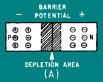
In figure 2-42, view (A), two materials are brought together to form a pn-junction diode. The different energy levels in the two materials cause a diffusion of the holes and electrons through both materials which tends to balance their energy levels. When this diffusion process stops, the diode is left with a small area on either side of the junction, called the depletion area, which contains no free electrons or holes. The movement of electrons through the materials creates an electric field across the depletion area that is described as a barrier potential and has the electrical characteristics of a charged capacitor.

Figure 2-42A. - Pn-junction diode as a variable capacitor.


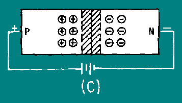
External bias, applied in either the forward or reverse direction, as shown in views (B) and (C) of figure 2-42, affects the magnitude, barrier potential, and width of the depletion area. Enough forward or reverse bias will overcome the barrier potential and cause current to flow through the diode. The width of the depletion region can be controlled by keeping the bias voltage at levels that do not allow current flow. Since the depletion area acts as a capacitor, the diode will perform as a variable capacitor that changes with the applied bias voltage. The capacitance of a typical varactor can vary from 2 to 50 picofarads for a bias variation of just 2 volts.

Figure 2-42B. - Pn-junction diode as a variable capacitor.


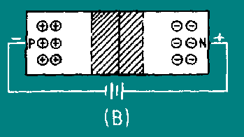
Figure 2-42C. - Pn-junction diode as a variable capacitor.


The variable capacitance property of the varactor allows it to be used in circuit applications, such as amplifiers, that produce much lower internal noise levels than circuits that depend upon resistance properties. Since noise is of primary concern in receivers, circuits using varactors are an important development in the field of low-noise amplification. The most significant use of varactors to date has been as the basic component in parametric amplifiers.


PARAMETRIC AMPLIFIERS. - The parametric amplifier is named for the time-varying parameter, or value of capacitance, associated with the operation. Since the underlying principle of operation is based on reactance, the parametric amplifier is sometimes called a REACTANCE AMPLIFIER.

The conventional amplifier is essentially a variable resistance that uses energy from a dc source to increase ac energy. The parametric amplifier uses a nonlinear variable reactance to supply energy from an ac source to a load. Since reactance does not add thermal noise to a circuit, parametric amplifiers produce much less noise than most conventional amplifiers.

Because the most important feature of the parametric amplifier is the low-noise characteristic, the nature of ELECTRONIC NOISE and the effect of this type of noise on receiver operation must first be discussed. Electronic noise is the primary limitation on receiver sensitivity and is the name given to very small randomly fluctuating voltages that are always present in electronic circuits. The sensitivity limit of the receiver is reached when the incoming signal falls below the level of the noise generated by the receiver circuits. At this point the incoming signal is hidden by the noise, and further amplification has no effect because the noise is amplified at the same rate as the signal. The effects of noise can be reduced by careful circuit design and control of operating conditions, but it cannot be entirely eliminated. Therefore, circuits such as the parametric amplifier are important developments in the fields of communication and radar.

The basic theory of parametric amplification centers around a capacitance that varies with time. Consider the simple series circuit shown in figure 2-43. When the switch is closed, the capacitor charges to value (Q). If the switch is opened, the isolated capacitor has a voltage across the plates determined by the charge Q divided by the capacitance C.


Figure 2-43. - Voltage amplification from a varying capacitor.


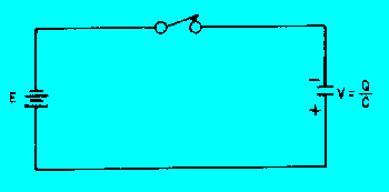
An increase in the charge Q or a decrease in the capacitance C causes an increase in the voltage across the plates. Thus, a voltage increase, or amplification, can be obtained by mechanically or electronically varying the amount of capacitance in the circuit. In practice a voltage-variable capacitance, such as a varactor, is used. The energy required to vary the capacitance is obtained from an electrical source called a PUMP.

Freddy Vallenilla EES Sec2

Two-Diode Odd-Order Frequency Multipliers


Two-Diode Odd-Order Frequency Multipliers


It is often necessary to multiply the frequency of low noise oscillators without significantly degrading the phase noise beyond the theoretical 20 log (N). Low noise frequency doublers constructed with Schottky signal diodes are readily available but higher-order multipliers often exhibit high flicker noise and poor noise floors due to the nature of the switching device. An odd-order diode multiplier topology published in RF Design magazine allows the use of low noise Schottky diodes to generate odd-order harmonics with very low excess noise. A new, half-wave version of the frequency multiplier is presented along with component values for constructing a 10 to 30 MHz tripler and a 10 to 50 MHz quintupler. The conversion loss for these multipliers is good considering their passive design and the input return loss may be easily optimized for different input levels. The circuit for the multiplier is shown below:


The input matching network consists of a choke and capacitor which work together to step up the voltage to overcome the diodes' barrier potential and to provide a low impedance to ground for the desired harmonic while preventing the harmonics form exiting the input. This series tank configuration gives the circuit a degree of feedback which helps to maintain a good conversion loss for a range of input levels. Diode, D1 rectifies the input signal resulting in a DC current in L4. The input signal commutates the two diodes with the result that a square wave of current flows in D2. The output network provides a low impedance to ground for the undesired frequencies and directs the desired harmonic to the output. Other networks may be used in the output circuit but the network should shunt undesired harmonics to preserve the fast diode switching and should block the larger, lower frequency harmonics. (Note: A current meter may be inserted in series with the ground leg of L4 to measure the DC diode current when prototyping.)

This basic configuration may be used for a wide range of frequencies with odd-order multiplication factors to 7 or more. Many fast-switching diode types may be used with excellent results and the choice will depend upon the signal levels and the required phase noise performance. Schottky-barrier diodes such as the 1N5711 are a good choice for most multiplier applications since the conversion efficiency is good and the phase noise performance is better than all but the best sources. Ordinary silicon switching diodes such as the 1N914 will give slightly better conversion efficiency for output frequencies up to 100 MHz but the phase noise performance may be significantly less than provided by Schottky diodes.

Figures 1 and 2 show the conversion loss for a 10 MHz input multiplied to 30 and 50 MHz. The conversion loss is quite low considering the multiplication factor and the 3x multiplier compares favorably with many frequency doublers.


C1 and L1 are selected to give good return loss for the level applied to the input of the multiplier and depends somewhat upon the diode type. Figures 3 and 4 show the return loss for various values of C1 and L1 for the two diode types. For example, if the input level is to be 10dBm, curve #2 would be selected since the return loss is near -30dB. The other component values are selected from the following chart:


C3 may be a 15pF trimmer capacitor for both designs and C2 may be a fixed value with a small trimmer in parallel. The Q of the C2-L2 tank is low and fixed components will usually suffice.


The output of these multipliers may be directly connected to an ordinary MMIC amplifier, if more output is necessary. Choose a low noise figure amplifier if the phase noise performance is critical. The multiplier's intrinsic phase noise can be quite good if constructed with low flicker Schottky diodes. Flicker intercept levels as low as -148 dBc have been realized with the noise floor projected to be near -180 dBc. Few oscillators will be degraded beyond theoretical amounts by such performance.

Freddy Vallenilla EES Sec2

The MOSFET


The MOSFET


As well as the Junction Field Effect Transistor, there is another type of Field Effect Transistor available whose Gate input is electrically insulated from the main current carrying channel and is therefore called an Insulated Gate Field Effect Transistor. The most common type of insulated gate FET or IGFET as it is sometimes called, is the Metal Oxide Semiconductor Field Effect Transistor or MOSFET for short.

The MOSFET type of field effect transistor has a "Metal Oxide" gate (usually silicon dioxide commonly known as glass), which is electrically insulated from the main semiconductor N-channel or P-channel. This isolation of the controlling gate makes the input resistance of the MOSFET extremely high in the Mega-ohms region and almost infinite. As the gate terminal is isolated from the main current carrying channel ""NO current flows into the gate"" and like the JFET, the MOSFET also acts like a voltage controlled resistor. Also like the JFET, this very high input resistance can easily accumulate large static charges resulting in the MOSFET becoming easily damaged unless carefully handled or protected.

Basic MOSFET Structure and Symbol


Metal Oxide Semiconductor FET


We also saw previously that the gate of a JFET must be biased in such a way as to forward-bias the PN junction but in a MOSFET device no such limitations applies so it is possible to bias the gate in either polarity. This makes MOSFET's specially valuable as electronic switches or to make logic gates because with no bias they are normally non-conducting and the high gate resistance means that very little control current is needed. Both the P-channel and the N-channel MOSFET is available in two basic forms, theEnhancement type and the Depletion type.

Depletion-mode MOSFET

The Depletion-mode MOSFET, which is less common than the enhancement types is normally switched "ON" without a gate bias voltage but requires a gate to source voltage (Vgs) to switch the device "OFF". Similar to the JFET types. For N-channel MOSFET's a "Positive" gate voltage widens the channel, increasing the flow of the drain current and decreasing the drain current as the gate voltage goes more negative. The opposite is also true for the P-channel types. The depletion mode MOSFET is equivalent to a "Normally Closed" switch.

Depletion-mode N-Channel MOSFET and circuit Symbols


Characteristics Curves for Depletion mode MOSFET

Circuit Symbols for Depletion mode MOSFET


Depletion-mode MOSFET's are constructed similar to their JFET transistor counterparts where the drain-source channel is inherently conductive with electrons and holes already present within the N-type or P-type channel. This doping of the channel produces a conducting path of low resistance between the drainand source with zero gate bias.

Enhancement-mode MOSFET

The more common Enhancement-mode MOSFET is the reverse of the depletion-mode type. Here the conducting channel is lightly doped or even undoped making it non-conductive. This results in the device being normally "OFF" when the gate bias voltage is equal to zero.

drain current will only flow when a gate voltage (Vgs) is applied to the gate terminal. This positive voltage creates an electrical field within the channel attracting electrons towards the oxide layer and thereby reducing the overall resistance of the channel allowing current to flow. Increasing this positive gate voltage will cause an increase in the drain current, Id through the channel. Then, the Enhancement-mode device is equivalent to a "Normally Open" switch.

Enhancement-mode N-Channel MOSFET and circuit Symbols


Characteristics Curves for Enhancement mode MOSFET

Circuit Symbols for Enhancement mode MOSFET


Enhancement-mode MOSFET's make excellent electronics switches due to their low "ON" resistance and extremely high "OFF" resistance and extremely high gate resistance.Enhancement-mode MOSFET's are used in integrated circuits to produce CMOS type Logic Gates and power switching circuits as they can be driven by digital logic levels.


MOSFET Summary

The MOSFET has an extremely high input gate resistance and as such a easily damaged by static electricity if not carefully protected. MOSFET's are ideal for use as electronic switches or common-source amplifiers as their power consumption is very small. Typical applications for MOSFET's are in Microprocessors, Memories, Calculators and Logic Gates etc. Also, notice that the broken lines within the symbol indicates a normally "OFF" Enhancement type showing that "NO" current can flow through the channel when zero gate voltage is applied and a continuous line within the symbol indicates a normally "ON" Depletion type showing that current "CAN" flow through the channel with zero gate voltage. For P-Channel types the symbols are exactly the same for both types except that the arrow points outwards.

This can be summarised in the following switching table.

MOSFET typeVgs = +veVgs = 0Vgs = -ve
N-Channel DepletionONONOFF
N-Channel EnhancementONOFFOFF
P-Channel DepletionOFFONON
P-Channel EnhancementOFFOFFON


Freddy Vallenilla EES Sec2

SOLID-STATE MICROWAVE DEVICES


SOLID-STATE MICROWAVE DEVICES

As with vacuum tubes, the special electronics effects encountered at microwave frequencies severely limit the usefulness of transistors in most circuit applications. The need for small-sized microwave devices has caused extensive research in this area. This research has produced solid-state devices with higher and higher frequency ranges. The new solid-state microwave devices are predominantly active, two-terminal diodes, such as tunnel diodes, varactors, transferred-electron devices, and avalanche transit-time diodes. This section will describe the basic theory of operation and some of the applications of these relatively new solid-state devices.

Tunnel Diode Devices

The TUNNEL DIODE is a pn junction with a very high concentration of impurities in both the p and n regions. The high concentration of impurities causes it to exhibit the properties of a negative-resistance element over part of its range of operation, as shown in the characteristic curve in figure 2-39. In other words, the resistance to current flow through the tunnel diode increases as the applied voltage increases over a portion of its region of operation. Outside the negative-resistance region, the tunnel diode functions essentially the same as a normal diode. However, the very high impurity density causes a junction depletion region so narrow that both holes and electrons can transfer across the pn junction by a quantum mechanical action called TUNNELING. Tunneling causes the negative-resistance action and is so fast that no transit-time effects occur even at microwave frequencies. The lack of a transit-time effect permits the use of tunnel diodes in a wide variety of microwave circuits, such as amplifiers, oscillators, and switching devices. The detailed theory of tunnel-diode operation and the negative-resistance property exhibited by the tunnel diode was discussed in NEETS, Module 7, Introduction to Solid-State Devices and Power Supplies, Chapter 3.

Figure 2-39. - Tunnel-diode characteristic curve.


TUNNEL-DIODE OSCILLATORS. - A tunnel diode, biased at the center point of the negative-resistance range (point B in figure 2-39) and coupled to a tuned circuit or cavity, produces a very stable oscillator. The oscillation frequency is the same as the tuned circuit or cavity frequency.

Microwave tunnel-diode oscillators are useful in applications that require microwatts or, at most, a few milliwatts of power, such as local oscillators for microwave superheterodyne receivers. Tunnel-diode oscillators can be mechanically or electronically tuned over frequency ranges of about one octave and have a top-end frequency limit of approximately 10 gigahertz.

Tunnel-diode oscillators that are designed to operate at microwave frequencies generally use some form of transmission line as a tuned circuit. Suitable tuned circuits can be built from coaxial lines, transmission lines, and waveguides.
An example of a highly stable tunnel-diode oscillator is shown in figure 2-40. A tunnel-diode is loosely coupled to a high-Q tunable cavity. Loose coupling is achieved by using a short, antenna feed probe placed off-center in the cavity. Loose coupling is used to increase the stability of the oscillations and the output power over a wider bandwidth.

Figure 2-40. - Tunnel-diode oscillator.


The output power produced is in the range of a few hundred microwatts, sufficient for many microwave applications. The frequency at which the oscillator operates is determined by the physical positioning of the tuner screw in the cavity. Changing the output frequency by this method is called MECHANICAL TUNING. In addition to mechanical tuning, tunnel-diode oscillators may be tuned electronically. One method is called BIAS TUNING and involves nothing more than changing the bias voltage to change the bias point on the characteristic curve of the tunnel-diode. Another method is called VARACTOR TUNING and requires the addition of a varactor to the basic circuit. Varactors were discussed in NEETS, Module 7, Introduction to Solid-State Devices, and Power Supplies, Chapter 3. Tuning is achieved by changing the voltage applied across the varactor which alters the capacitance of the tuned circuit.


TUNNEL-DIODE AMPLIFIERS. - Low-noise, tunnel-diode amplifiers represent an important microwave application of tunnel diodes. Tunnel-diode amplifiers with frequencies up to 85 gigahertz have been built in waveguides, coaxial lines, and transmission lines. The low-noise generation, gain ratios of up to 30 dB, high reliability, and light weight make these amplifiers ideal for use as the first stage of amplification in communications and radar receivers.

Most microwave tunnel-diode amplifiers are REFLECTION-TYPE, CIRCULATOR-COUPLED AMPLIFIERS. As in oscillators, the tunnel diode is biased to the center point of its negative-resistance region, but a CIRCULATOR replaces the tuned cavity.

A circulator is a waveguide device that allows energy to travel in one direction only, as shown in figure 2-41. The tunnel diode in figure 2-41 is connected across a tuned-input circuit. This arrangement normally produces feedback that causes oscillations if the feedback is allowed to reflect back to the tuned-input circuit. The feedback is prevented because the circulator carries all excess energy to the absorptive load (RL). In this configuration the tunnel diode cannot oscillate, but will amplify.

Figure 2-41. - Tunnel-diode amplifier.


The desired frequency input signal is fed to port 1 of the circulator through a bandpass filter. The filter serves a dual purpose as a bandwidth selector and an impedance-matching device that improves the gain of the amplifiers. The input energy enters port 2 of the circulator and is amplified by the tunnel diode. The amplified energy is fed from port 2 to port 3 and on to the mixer. If any energy is reflected from port 3, it is passed to port 4, where it is absorbed by the matched load resistance.


TUNNEL-DIODE FREQUENCY CONVERTERS AND MIXERS. - Tunnel diodes make excellent mixers and frequency converters because their current-voltage characteristics are highly nonlinear. While other types of frequency converters usually have a conversion power loss, tunnel-diode converters can actually have a conversion power gain. A single tunnel diode can also be designed to act as both the nonlinear element in a converter and as the negative-resistance element in a local oscillator at the same time.

Practical tunnel-diode frequency converters usually have either a unity conversion gain or a small conversion loss. Conversion gains as high as 20 dB are possible if the tunnel diode is biased near or into the negative-resistance region. Although high gain is useful in some applications, it presents problems in stability. For example, the greatly increased sensitivity to variations in input impedance can cause high-gain converters to be unstable unless they are protected by isolation circuitry.
As with tunnel-diode amplifiers, low-noise generation is one of the more attractive characteristics of tunnel-diode frequency converters. Low-noise generation is a primary concern in the design of today's extremely sensitive communications and radar receivers. This is one reason tunnel-diode circuits are finding increasingly wide application in these fields.

Freddy Vallenilla EES Sec2

Junction Field Effect Transistor

Junction Field Effect Transistor


The common transistor is called a junction transistor, and it was the key device which led to the solid state electronics revolution. In application, the junction transistor has the disadvantage of a low input impedance because the base of the transistor is the signal input and the base-emitter diode is forward biased. Another device achieved transistor action with the input diode junction reversed biased, and this device is called a "field effect transistor" or a "junction field effect transistor", JFET. With the reverse biased input junction, it has a very high input impedance. Having a high input impedance minimizes the interference with or "loading" of the signal source when a measurement is made.

      For an n-channel FET, the device is constructed from a bar of n-type material, with the shaded areas
      composed of a p-type material as a Gate. Between the Source and the Drain, the n-type material acts as a 
      resistor. The current flow consists of the majority carriers (electrons for n-type material).


Since the Gate junction is reverse biased and because there is no minority carrier contribution to the flow through the device, the input impedance is extremely high.

The control element for the JFET comes from depletion of charge carriers from the n-channel. When the Gate is made more negative, it depletes the majority carriers from a larger depletion zone around the gate. This reduces the current flow for a given value of Source-to-Drain voltage. Modulating the Gate voltage modulates the current flow through the device.


JFET Characteristic Curves


Characteristic curves for the JFETare shown at left. You can see that for a given value of Gate voltage, the current is very nearly constant over a wide range of Source-to-Drain voltages. The control element for the JFET comes from depletion of charge carriers from the n-channel. When the Gate is made more negative, it depletes the majority carriers from a larger depletion zone around the gate. This reduces the current flow for a given value of Source-to-Drain voltage. Modulating the Gate voltage modulates the current flow through the device.


The transfer characteristic for the JTET is useful for visualizing the gain from the device and identifying the region of linearity. The gain is proportional to the slope of the transfer curve. The current value IDSS represents the value when the Gate is shorted to ground, the maximum current for the device. This value will be part of the data supplied by the manufacturer. The Gate voltage at which the current reaches zero is called the "pinch voltage", VP. Note that the dashed line representing the gain in the linear region of operation strikes the zero current line at about half the pinch voltage.


IGFET


The insulated gate field effect transistor (IGFET) differs from the JFET by the addition of a silicon dioxide layer over the JFET and then a layer of silicon nitride. The result is a device which has even higher input impedance. The goal of extremely high input impedance allows an amplifier to sample some signal with minimal "loading" or interference with the signal source.
Common devices using this strategy are called MOSFETs, for metal oxide field effect transistors. They have achieved input impedances on the order of 1015 ohms.


Common Source JFET Amplifier


The most frequently encountered configuration for a JFET amplifier is the common source circuit. The source is common to the input and output as shown in the diagram.


Freddy Vallenilla EES Sec2

HEMT, High electron mobility transistor


HEMT, High electron mobility transistor


Summary or tutorial of the basics of the High Electron Mobility Transistor, HEMT, used in many RF design applications and RF circuits.


The HEMT or High Electron Mobility Transistor is a form of field effect transistor (FET) that is used to provide very high levels of performance at microwave frequencies. It offers a combination of low noise figure combined with the ability to operate at the very high microwave frequencies. Accordingly the HEMT is used in areas of RF design where high performance is required at very high RF frequencies.
The development of the HEMT took many years. It was not until many years after the basic FET was established as a standard electronics component that the HEMT appeared on the market. The specific mode of carrier transport used in HEMTs was first investigated in 1969, but it was not until 1980 that the first experimental devices were available for the latest RF design projects. During the 1980s they started to be used, but in view of their initial very high cost their use was considerably limited. Now with their cost somewhat less, they are more widely used, even finding uses in the mobile telecommunications as well as a variety of microwave radio communications links, and many other RF design applications.

HEMT construction

The key element within a HEMT is the specialised PN junction that it uses. It is known as a hetero-junction and consists of a junction that uses different materials either side of the junction. The most common materials used aluminium gallium arsenide (AlGaAs) and gallium arsenide (GaAs). Gallium arsenide is generally used because it provides a high level of basic electron mobility and this is crucial to the operation of the device. Silicon has a much lower level of electron mobility and as a result it is never used in a HEMT.
There is a variety of different structures that can be used within a HEMT, but all use basically the same manufacturing processes.
In the manufacture of a HEMT, first an intrinsic layer of gallium arsenide is set down on the semi-insulating gallium arsenide layer. This is only about one micron thick. About one micron thick is set down. Next a very thin layer between 30 and 60 Angstroms of intrinsic aluminium gallium arsenide is set down on top of this. Its purpose is to ensure the separation of the hetero-junction interface from the doped aluminium gallium arsenide region. This is critical if the high electron mobility is to be achieved. The doped layer of aluminium gallium arsenide about 500 Angstroms thick is set down above this as shown in the diagrams. Precise control of the thickness of this layer is required and special techniques are required for the control of this.
There are two main structures that are used. These are the self aligned ion implanted structure and the recess gate structure. In the case of the self aligned ion implanted structure the gate, drain and source are set down and are generally metallic contacts, although source and drain contacts may sometimes be made from germanium. The gate is generally made from titanium, and it forms a minute reverse biased junction similar to that of the GaAsFET.
For the recess gate structure another layer of n-type gallium arsenide is set down to enable the drain and source contacts to be made. Areas are etched as shown in the diagram. The thickness under the gate is also very critical since the threshold voltage of the FET is determined by this. The size of the gate, and hence the channel is very small. Typically the gate is only 0.25 microns or less, enabling the device to have a very good high frequency performance.

HEMT operation

The operation of the HEMT is somewhat different to other types of FET and as a result it is able to give a very much improved performance over the standard junction or MOS FETs, and in particular in microwave radio applications.
Electrons from the n-type region move through the crystal lattice and many remain close to the hetero-junction. These electrons for a layer that is only one layer thick forming what is known as a two dimensional electron gas. Within this region the electrons are able to move freely because there are no other donor electrons or other items with which electrons will collide and the mobility of the electrons in the gas is very high.
A bias applied to the gate formed as a schottky barrier diode is used to modulate the number of electrons in the channel formed from the 2 D electron gas and in turn this controls the conductivity of the device. This can be compared to the more traditional types of FET where the width of the channel is changed by the gate bias.

Applications

The HEMT was originally developed for high speed applications. It was only when the first devices were fabricated that it was discovered they exhibited a very low noise figure. This is related to the nature of the two dimensional electron gas and the fact that there are less electron collisions.
As a result of their noise performance they are widely used in low noise small signal amplifiers, power amplifiers, oscillators and mixers operating at frequencies up to 60 GHz and more and it is anticipated that ultimately devices will be widely available for frequencies up to about 100 GHz. In fact HEMT devices are used in a wide range of RF design applications including cellular telecommunications, Direct broadcast receivers - DBS, radar, radio astronomy, and any RF design application that requires a combination of low noise and very high frequency performance
HEMTs are manufactured by many semiconductor device manufacturers around the globe. They may be in the form of discrete transistors, but nowadays they are more usually incorporated into integrated circuits. These Monolithic Microwave Integrated Circuit chips, or MMICs are widely used for RF design applications, and HEMT based MMICs are widely used to provide the required level of performance in many areas.

PHEMT

A further development of the HEMT is known as the PHEMT. PHEMTs, Pseudomorphic High Electron Mobility Transistors are extensively used in wireless communications and LNA applications. PHEMT transistors find wide market acceptance because of their high power added efficiencies and excellent low noise figures and performance. As a result, PHEMTs are widely used in satellite communication systems of all forms including including direct broadcast satellite television, DBS-TV, where they are used in the low noise boxes, LNBs used with the satellite antennas. They are also widely used in general satellite communication systems as well as radar and microwave radio communications systems. PHEMT technology is also used in high-speed analogue and digital IC technology where exceedingly high speed is required.
 Freddy Vallenilla EES Sec 2

HEMT, High electron mobility transistor


HEMT, High electron mobility transistor


Summary or tutorial of the basics of the High Electron Mobility Transistor, HEMT, used in many RF design applications and RF circuits.


The HEMT or High Electron Mobility Transistor is a form of field effect transistor (FET) that is used to provide very high levels of performance at microwave frequencies. It offers a combination of low noise figure combined with the ability to operate at the very high microwave frequencies. Accordingly the HEMT is used in areas of RF design where high performance is required at very high RF frequencies.
The development of the HEMT took many years. It was not until many years after the basic FET was established as a standard electronics component that the HEMT appeared on the market. The specific mode of carrier transport used in HEMTs was first investigated in 1969, but it was not until 1980 that the first experimental devices were available for the latest RF design projects. During the 1980s they started to be used, but in view of their initial very high cost their use was considerably limited. Now with their cost somewhat less, they are more widely used, even finding uses in the mobile telecommunications as well as a variety of microwave radio communications links, and many other RF design applications.

HEMT construction

The key element within a HEMT is the specialised PN junction that it uses. It is known as a hetero-junction and consists of a junction that uses different materials either side of the junction. The most common materials used aluminium gallium arsenide (AlGaAs) and gallium arsenide (GaAs). Gallium arsenide is generally used because it provides a high level of basic electron mobility and this is crucial to the operation of the device. Silicon has a much lower level of electron mobility and as a result it is never used in a HEMT.
There is a variety of different structures that can be used within a HEMT, but all use basically the same manufacturing processes.
In the manufacture of a HEMT, first an intrinsic layer of gallium arsenide is set down on the semi-insulating gallium arsenide layer. This is only about one micron thick. About one micron thick is set down. Next a very thin layer between 30 and 60 Angstroms of intrinsic aluminium gallium arsenide is set down on top of this. Its purpose is to ensure the separation of the hetero-junction interface from the doped aluminium gallium arsenide region. This is critical if the high electron mobility is to be achieved. The doped layer of aluminium gallium arsenide about 500 Angstroms thick is set down above this as shown in the diagrams. Precise control of the thickness of this layer is required and special techniques are required for the control of this.
There are two main structures that are used. These are the self aligned ion implanted structure and the recess gate structure. In the case of the self aligned ion implanted structure the gate, drain and source are set down and are generally metallic contacts, although source and drain contacts may sometimes be made from germanium. The gate is generally made from titanium, and it forms a minute reverse biased junction similar to that of the GaAsFET.
For the recess gate structure another layer of n-type gallium arsenide is set down to enable the drain and source contacts to be made. Areas are etched as shown in the diagram. The thickness under the gate is also very critical since the threshold voltage of the FET is determined by this. The size of the gate, and hence the channel is very small. Typically the gate is only 0.25 microns or less, enabling the device to have a very good high frequency performance.

HEMT operation

The operation of the HEMT is somewhat different to other types of FET and as a result it is able to give a very much improved performance over the standard junction or MOS FETs, and in particular in microwave radio applications.
Electrons from the n-type region move through the crystal lattice and many remain close to the hetero-junction. These electrons for a layer that is only one layer thick forming what is known as a two dimensional electron gas. Within this region the electrons are able to move freely because there are no other donor electrons or other items with which electrons will collide and the mobility of the electrons in the gas is very high.
A bias applied to the gate formed as a schottky barrier diode is used to modulate the number of electrons in the channel formed from the 2 D electron gas and in turn this controls the conductivity of the device. This can be compared to the more traditional types of FET where the width of the channel is changed by the gate bias.

Applications

The HEMT was originally developed for high speed applications. It was only when the first devices were fabricated that it was discovered they exhibited a very low noise figure. This is related to the nature of the two dimensional electron gas and the fact that there are less electron collisions.
As a result of their noise performance they are widely used in low noise small signal amplifiers, power amplifiers, oscillators and mixers operating at frequencies up to 60 GHz and more and it is anticipated that ultimately devices will be widely available for frequencies up to about 100 GHz. In fact HEMT devices are used in a wide range of RF design applications including cellular telecommunications, Direct broadcast receivers - DBS, radar, radio astronomy, and any RF design application that requires a combination of low noise and very high frequency performance
HEMTs are manufactured by many semiconductor device manufacturers around the globe. They may be in the form of discrete transistors, but nowadays they are more usually incorporated into integrated circuits. These Monolithic Microwave Integrated Circuit chips, or MMICs are widely used for RF design applications, and HEMT based MMICs are widely used to provide the required level of performance in many areas.

PHEMT

A further development of the HEMT is known as the PHEMT. PHEMTs, Pseudomorphic High Electron Mobility Transistors are extensively used in wireless communications and LNA applications. PHEMT transistors find wide market acceptance because of their high power added efficiencies and excellent low noise figures and performance. As a result, PHEMTs are widely used in satellite communication systems of all forms including including direct broadcast satellite television, DBS-TV, where they are used in the low noise boxes, LNBs used with the satellite antennas. They are also widely used in general satellite communication systems as well as radar and microwave radio communications systems. PHEMT technology is also used in high-speed analogue and digital IC technology where exceedingly high speed is required.

Freddy Vallenilla EES Sec