Pushing AlInN and AlGaN HEMTs further on SiC and silicon
The Terahertz Electronics Group of the Swiss Federal Institute of Technology Zurich (ETH-Zürich) has made progress, collaborating with other groups, in producing nitride semiconductor high-electron-mobility transistors (HEMTs) with performance characteristics beyond 100GHz (0.1THz). The group believes that such components could lead to high-power and high-speed performance, even in higher-temperature environments.
With Institute of Quantum Electronics and Photonics, Ecole Polytechnique Fédérale de Lausanne (EPFL), aluminum indium nitride on gallium nitride (AlInN/GaN) devices with a cut-off frequency (fT) of 144GHz with 100nm gate length have been developed on semi-insulating silicon carbide (SiC) substrates [Haifeng Sun et al, IEEE Electron Device Letters, published online 22 February 2010]. Using high-resistivity (111) silicon (HR-Si, 20kΩ-cm) substrates and a similar device structure, the same research achieved an fT of 113GHz. Looking to lower costs, AlGaN/GaN devices on high-resistivity (111) Si (10kΩ-cm) substrates have also been developed with Nitronex, exhibiting an fT of 107GHz [Stefano Tirelli et al, IEEE Electron Device Letters, published online 25 February 2010].
The ETH-Zürich/EPFL work used the newer, less mature AlInN/GaN heterojunction since this format is predicted to yield higher transconductance and current density values compared with AlGaN/GaN heterojunctions. The AlInN layers can be more nearly lattice matched with GaN, compared with AlGaN/GaN. While initial work has confirmed the expectations of better transconductance and current density, the frequency bandwidth performance has previously lagged behind the AlGaN/GaN reports. Now, the ETH-Zürich/EPFL team has not only beaten the previous fT high of 102GHz for AlInN/GaN devices with 100nm gate length, it has also managed to match the best published values for AlGaN/GaN HEMTs, even those with an insulated gate.
The metal-organic chemical vapor deposition (MOCVD) growth of the epitaxial layers on the respective substrates was carried out at EPFL: beginning with a 30nm aluminum nitride (AlN) nucleation layer, 1μm GaN insulating buffer and channel, 1nm AlN spacer, and finishing with a 10nm Al0.83In0.17N barrier. The SiC epitaxial wafers had channel electron sheet densities of 2.4x10¹³/cm2 and mobility of 1300cm 2/V-s, measured using the Hall effect. The corresponding values for the HR-Si structures were 1.95x10¹³/cm2 and mobility of 1060cm 2/V-s, respectively.
The resulting sheet resistances were 200Ω/sq (SiC) and 300Ω/sq (HR-Si), improving the values from the group's previous work by 2–3x. This has been enabled by improving the material quality, particularly at the AlInN/GaN interface. This was achieved by optimizing the buffer layer thickness and the growth temperatures.
Devices were formed using chlorine/methane/helium/argon plasma to etch 200nm isolation mesas and evaporating titanium/aluminum/gold (Ti/Al/Au) ohmic source/drain contacts (resistances of 0.48Ω-mm on SiC, 0.49Ω-mm on HR-Si). The 100nm T-gates of nickel/gold (Ni/Au) were formed using electron-beam lithography and lift-off techniques. A 100nm plasma-enhanced CVD silicon nitride passivation was used, along with Ti/Au overlay metallization on the ohmic and gate metal contacts.
The maximum drain current for a 2x(0.1x75μm) device on SiC was 1.84A/mm with zero gate–source potential difference (VGS = 0V), while the maximum extrinsic transconductance was 480mS/mm (VDS = 4V).
Complete channel pinch-off was not achieved due to residual gate leakage. Buffer leakage is excluded as the reason for the soft pinch-off by the experimenters due to the high isolation between the mesas (greater than 1010Ω/sq). Gate leakage is commonly observed in AlInN/GaN HEMTs with thin AlInN barrier layers. The reasons for the gate leakage are being investigated; the researchers would also like to find a suitable gate insulator, as opposed to using a Schottky contact with the AlInN barrier. The maximum current and extrinsic transconductance for similar HR-Si devices were 1.43A/mm and 335mS/mm with the same bias conditions.
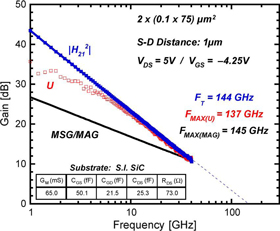
Microwave
performance for
2 x (0.1x75μm)
AlInN/GaN
HEMTs on SiC (a - right)
and HR-Si (b - below)
produced by
ETH-Zürich/EPFL.
Extrapolations at –20dB/dec.
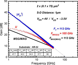 Radio-frequency measurements were carried out from DC to 40GHz (Figure 1). Measurements with VDS of 5V and VGS of -4.25V give, in addition to the fT value of 144GHz, a maximum oscillation frequency of 137GHz (fMAX(U)) based on extrapolation of Mason's unilateral gain (145GHz for maximum available gain, fMAX(MAG)). The HR-Si values were 113GHz (fT), 105GHz (f MAX(U)) and 113GHz (fMAX(MAG)) at VDS of 4V and VGS of -3.5V.
The ETH-Zürich/Nitronex work involved AlGaN/GaN/Si epitaxial wafers grown at Nitronex' facility. The base 100mm-diameter substrate was a high-resistivity (111) Si (10kΩ-cm) substrate. The insulating buffer/channel GaN was 1.7μm thick. The barrier layer was 17.5nm Al0.26Ga0.74N. A 2nm GaN cap layer was also deposited. The resulting mobility was about 1500cm2/V-s. HEMT devices were constructed with mesa isolation, Ti/Al/Au ohmic contacts, and Ni/Au T-gate lengths of 75nm and 100nm (200nm and 400nm T-heads, respectively). The source–drain distances were 2μm and 1μm for the 75nm and 100nm gate-length devices, respectively. SiN passivation of 100nm thickness was applied with PECVD and Ti/Au overlay metal with evaporation/lift-off.
The maximum drain current and extrinsic transconductance (VDS = 3V) were 705mA/mm and 285mS/mm, respectively, for the 75nm gate length. The respective figures for the 100nm device were 750mA/mm and 310mS/mm. The lower 75nm values were attributed to the large source–drain distance. Complete channel pinch-off was achieved at VGS values of -3.5V and -3.3V for the 75nm and 100nm devices, respectively. The breakdown characteristics BVGD, with a current threshold of 1mA/mm, were 58V and 30V for 75nm and 100nm devices, respectively. The shorter source–drain distance in the latter case increases the electric field in the device.
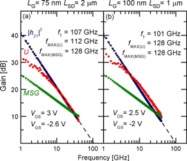
Figure 2:
Microwave
performance for
75nm (a) and
100nm (b) for
AlGaN/GaN
HEMTs produced
by ETH-Zürich/Nitronex.
Extrapolations at –20dB/dec.
RF measurements were carried out between 0.2GHz and 40.2GHz. These revealed fMAX(MSG)/fT values of 128GHz/107GHz and 128GHz/101GHz for the 75nm and 100nm HEMTs, respectively (Figure 2). According to the authors, these results supersede previous records for such devices built on HR-Si substrates. 'The peak fT = 107GHz with the LG = 75 nm gate HEMT is, to the best of our knowledge, the highest cutoff frequency value ever reported for fully passivated (Al,Ga)N/GaN or (Al,In)N/GaN HEMTs on HR-Si.' [The ETH-Zürich/Nitronex paper was submitted about two weeks before the ETH-Zürich/EPFL work discussed above.] The results also compare favorably with similar devices built on more traditional SiC substrates.
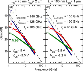
Figure 3:
Microwave
performance with
increased drain
bias for 75nm (a)
and 100nm (b)
for AlGaN/GaN
HEMTs produced
by ETH-Zürich/Nitronex.
Extrapolations at –20dB/dec.
The maximum oscillation frequency can be increased from the 128GHz value with a higher drain voltage (Figure 3): the 75nm device can reach 148GHz (fMAX(MSG), fMAX(U) = 128GHz); and the 100nm HEMT gives 150GHz (and also fMAX(U) = 150GHz). These are 'unprecedented' values for HR-Si devices with fT more than 90GHz (although not for SiC-based components with no or ultrathin passivation).
Freddy Vallenilla EES Sec 2
No hay comentarios:
Publicar un comentario