sábado, 26 de junio de 2010

Heterojunction Bipolar Transistor


The first SiGe device to go into production was the HBT in 1999. The performance of a Si bipolar (BJT) can be enhanced by the addition of SiGe to the base region of the transistor. Two schemes exist to enhance performance, a rectangular Ge base profile (HBT) and a linearly graded base. The linear base provides a built in electric field which accelerates electrons across the base region. The band structure for the HBT and the linear grade transistors are shown on the right.

The demonstrated cutoff frequencies (fT - the frequency where the gain for the transistor equals 1) for HBTs has now reached 360 GHz and this is predicted to increase as technology progresses. There is a downside to this, however, in that the breakdown voltage between the collector and the emitter also decreases as fT is increased.

Freddy R Vallenilla R
16.791.006
EES SEC 2

Varactors


varactor is also known as a variable capacitance diode or a varicap. It provides an electrically controllable capacitance, which can be used in tuned circuits. It is small and inexpensive, which makes its use advantageous in many applications. Its disadvantages compared to a manually controlled variable capacitor are a lower Q, nonlinearity, lower voltage rating and a more limited range. Background material on varactors can be found in the Reference.


Any PN junction has a junction capacitance that is a function of the voltage across the junction, as discussed in any account of PN junctions. The electric field in the depletion layer that is set up by the ionized donors and acceptors is responsible for the voltage difference that balances the applied voltage. A higher reverse bias widens the depletion layer, uncovering more fixed charge and raising the junction potential. The capacitance of the junction is C = Q(V)/V, and the incremental capacitance is c = dQ(V)/dV. The capacitance to be used in the formula for the resonant frequency is the incremental capacitance, where it is assumed that the voltage excursions dV are small compared to V. Finite voltages give rise to nonlinearities. Efforts may be made to reduce these nonlinearities in some cases.

The capacitance decreases as the reverse bias increases, according to the relation C = Co/(1 + V/Vo)n, where Co and Vo are constants. Vo is approximately the forward voltage of the diode. The exponent n depends on how the doping density of the semiconductors depend on distance away from the junction. For a graded junction (linear variation), n = 0.33. For an abrupt junction (constant doping density), n = 0.5. If the density jumps abruptly at the junction, then decreases (called hyperabrupt), n can be made as high as n = 2. I expect that the doping on one side of the junction is heavy, and the depletion layer is predominately on one side, but this is a constructional detail.

Availability of Varactors

For the experiments described below, I used some varactors that were furnished by a surplus house. These were in the TO-92 package that is so convenient for experiments, and came in matched sets of three. A look in the Digi-Key catalog revealed that although a variety of varactors from Zetex are available and inexpensive (p. 398), they are available only in the SOT-23 surface-mount package. This is another example of how things are becoming more difficult for those trying to learn about electronics.

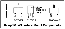
The solution for this problem is offered by the "Surfboards" of Capital Advanced Technologies (p. 752). These are small boards, as shown at the right, with SIP pins (inline pins at 0.1" spacing) and pads suitable for surface-mount devices. Discrete devices, like our SOT-23 diodes, can be easily soldered to the 6000-series Surfboards. The 6103CA, which holds one device, is suitable. The connections are shown at the right. If you buy your Surfboards from Digi-Key, you will get instructions on how to use them. The methods described here can also be used with surface-mount transistors and components, which will also fit on the Surfboards. This seems to be a practical way to use surface-mount devices when you are compelled to do so.

I used the following tools: a 12W fine-tip soldering iron (Weller WM120); .025" dia. 60/40 rosin-core solder; fine-point tweezers; a round toothpick; clear household cement; a 10X magnifier for inspection; and, finally, a bright light. Remove the diode by pulling off the clear tape on the carrier. The SOT-23 package is seriously tiny! Make sure you can recognize top and bottom. Lay the 6103CA face-up. Put a small drop of cement on the end of the toothpick, and deposit a tiny amount at the point where the package will be attached. Then place the package on the dot of cement with the tweezers, with its feet in the proper places, and press down. This holds the package while it is being soldered, and is a step that should not be omitted. The tip of the soldering iron should be tinned. Touch the solder to the tip so that a small drop is left hanging on the tip. Now, very carefully bring the drop into contact with the pad of the package and the foil of the 6103CA board at one of the feet of the SOT-23. Capillary attraction will soon cause the solder to spread in the usual way. Press down lightly to ensure that the package is seated. This all takes only a second. Examine the joints with a 10X magnifier to make sure that the feet are entangled in the solder. It's a good idea to put a label on the back of the 6103 to identify the part, since the SOT-23 package is too small for identification.

Experiments

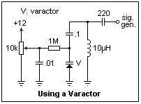
The basic circuit for testing a varactor is shown at the right. The key is the 1M resistor that isolates the DC voltage source from the circuit attached to the varactor. The 0.1μF capacitor blocks the DC bias voltage. I happened to have a 10μH inductor at hand, one of those that looks like a fat resistor, and has a reasonably high Q. The RF signal generator was coupled through a 220pF capacitor, and set for an unmodulated output. Because of stray capacitances, we cannot accurately measure the capacitance of the varactor with this circuit, but we can certainly see its action.
A capacitance meter did not give satisfactory results, so another method closely related to the actual application of the varactor was used. While observing the voltage across the tuned circuit with an oscilloscope, I varied the frequency looking for a maximum. From the resonant frequency, I then calculated the capacitance using the usual formula.


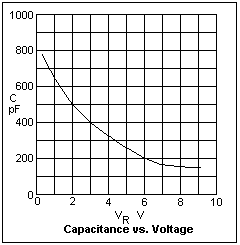
The results of a series of measurements is shown at the left. The capacitance varied from about 170 pF at 8 V to 750 pF at 0.5V, a satisfactory range. If you plot the frequency vs. the voltage, the result is almost linear, showing that the varactor is of the hyperabrupt type, since n = 2 will give frequency proportional to voltage. I also determined that the MPN3404 that I found in the varactor drawer was probably not a varactor. It was not described, but was listed, in the Motorola data book.
Further experiments will be described, with applications, when I obtain some more varactors.


Freddy R Vallenilla R
16.791.006
EES SEC 2

The Transistor as a Switch


When used as an AC signal amplifier, the transistors Base biasing voltage is applied so that it operates within its "Active" region and the linear part of the output characteristics curves are used. However, both the NPN & PNP type bipolar transistors can be made to operate as an "ON/OFF" type solid state switch for controlling high power devices such as motors, solenoids or lamps. If the circuit uses the Transistor as a Switch, then the biasing is arranged to operate in the output characteristics curves seen previously in the areas known as the "Saturation" and "Cut-off" regions as shown below.

Transistor Curves


Transistor Curves for Switching

The pink shaded area at the bottom represents the "Cut-off" region. Here the operating conditions of the transistor are zero input base current (Ib), zero output collector current (Ic) and maximum collector voltage (Vce) which results in a large depletion layer and no current flows through the device. The transistor is switched "Fully-OFF". The lighter blue area to the left represents the "Saturation" region. Here the transistor will be biased so that the maximum amount of base current is applied, resulting in maximum collector current flow and minimum collector emitter voltage which results in the depletion layer being as small as possible and maximum current flows through the device. The transistor is switched "Fully-ON". Then we can summarize this as:
  • 1. Cut-off Region - Both junctions are Reverse-biased, Base current is zero or very small resulting in zero Collector current flowing, the device is switched fully "OFF".
  •  
  • 2. Saturation Region - Both junctions are Forward-biased, Base current is high enough to give a Collector-Emitter voltage of 0v resulting in maximum Collector current flowing, the device is switched fully "ON".
An example of an NPN Transistor as a switch being used to operate a relay is given below. With inductive loads such as relays or solenoids a flywheel diode is placed across the load to dissipate the back EMF generated by the inductive load when the transistor switches "OFF" and so protect the transistor from damage. If the load is of a very high current or voltage nature, such as motors, heaters etc, then the load current can be controlled via a suitable relay as shown.

Transistor Switching Circuit


Transistor Switch

The circuit resembles that of the Common Emitter circuit we looked at in the previous tutorials. The difference this time is that to operate the transistor as a switch the transistor needs to be turned either fully "OFF" (Cut-off) or fully "ON" (Saturated). An ideal transistor switch would have an infinite resistance when turned "OFF" resulting in zero current flow and zero resistance when turned "ON", resulting in maximum current flow. In practice when turned "OFF", small leakage currents flow through the transistor and when fully "ON" the device has a low resistance value causing a small saturation voltage (Vce) across it. In both the Cut-off and Saturation regions the power dissipated by the transistor is at its minimum.

To make the Base current flow, the Base input terminal must be made more positive than the Emitter by increasing it above the 0.7 volts needed for a silicon device. By varying the Base-Emitter voltage Vbe, the Base current is altered and which in turn controls the amount of Collector current flowing through the transistor as previously discussed. When maximum Collector current flows the transistor is said to beSaturated. The value of the Base resistor determines how much input voltage is required and corresponding Base current to switch the transistor fully "ON".

Example No1.

For example, using the transistor values from the previous tutorials of:   β = 200, Ic = 4mA and Ib = 20uA, find the value of the Base resistor (Rb) required to switch the load "ON" when the input terminal voltage exceeds 2.5v.

Switch Example 1

Example No2.

Again using the same values, find the minimum Base current required to turn the transistor fully "ON" (Saturated) for a load that requires 200mA of current.

Switch Example 2

Transistor switches are used for a wide variety of applications such as interfacing large current or high voltage devices like motors, relays or lamps to low voltage digital logic IC's or gates like AND Gates or ORGates. Here, the output from a digital logic gate is only +5v but the device to be controlled may require a 12 or even 24 volts supply. Or the load such as a DC Motor may need to have its speed controlled using a series of pulses (Pulse Width Modulation) and transistor switches will allow us to do this faster and more easily than with conventional mechanical switches.

Digital Logic Transistor Switch


Digital Logic Transistor Switch

The base resistor, Rb is required to limit the output current of the logic gate.

Darlington Transistors

Sometimes the DC current gain of the bipolar transistor is too low to directly switch the load current or voltage, so multiple switching transistors are used. Here, one small input transistor is used to switch "ON" or "OFF" a much larger current handling output transistor. To maximise the signal gain the two transistors are connected in a "Complementary Gain Compounding Configuration" or what is generally called a "Darlington Configuration" where the amplification factor is the product of the two individual transistors.

Darlington Transistors simply contain two individual bipolar NPN or PNP type transistors connected together so that the current gain of the first transistor is multiplied with that of the current gain of the second transistor to produce a device which acts like a single transistor with a very high current gain. The overall current gain Beta (β) or Hfe value of a Darlington device is the product of the two individual gains of the transistors and is given as:

Darlington Transistor Current Gain

So Darlington Transistors with very high β values and high Collector currents are possible compared to a single transistor. An example of the two basic types of Darlington transistor are given below.

Darlington Transistor Configurations


Darlington Transistor


The above NPN Darlington transistor configuration shows the Collectors of the two transistors connected together with the Emitter of the first transistor connected to the Base of the second transistor therefore, the Emitter current of the first transistor becomes the Base current of the second transistor. The first or "input" transistor receives an input signal, amplifies it and uses it to drive the second or "output" transistors which amplifies it again resulting in a very high current gain. As well as its high increased current and voltage switching capabilities, another advantage of a Darlington transistor is in its high switching speeds making them ideal for use in Inverter circuits and DC motor or stepper motor control applications.

One difference to consider when using Darlington transistors over the conventional single bipolar transistor type is that the Base-Emitter input voltage Vbe needs to be higher at approx 1.4v for silicon devices, due to the series connection of the two PN junctions.

Then to summarise when using a Transistor as a Switch.
  • Transistor switches can be used to switch and control lamps, relays or even motors.
  • When using bipolar transistors as switches they must be fully "OFF" or fully "ON".
  • Transistors that are fully "ON" are said to be in their Saturation region.
  • Transistors that are fully "OFF" are said to be in their Cut-off region.
  • In a transistor switch a small Base current controls a much larger Collector current.
  • When using transistors to switch inductive relay loads a "Flywheel Diode" is required.
  • When large currents or voltages need to be controlled, Darlington Transistors are used.

The Schottky barrier diode


The Schottky diode or Schottky Barrier diode is an electronics component that is widely used for radio frequency (RF) applications as a mixer or detector diode. 
The Schottky diode is also used in power applications as a rectifier, again because of its low forward voltage drop leading to lower levels of power loss compared to ordinary PN junction diodes. Although normally called the Schottky diode these days, named after Schottky, it is also sometimes referred to as the surface barrier diode, hot carrier diode or even hot electron diode.
Despite the fact that Schottky barrier diodes have many applications in today's high tech electronics scene, it is actually one of the oldest semiconductor devices in existence. As a metal-semiconductor devices, its applications can be traced back to before 1900 where crystal detectors, cat's whisker detectors and the like were all effectively Schottky barrier diodes.


Structure

The Schottky barrier diode can be manufactured in a variety of forms. The most simple is the point contact diode where a metal wire is pressed against a clean semiconductor surface. This was how the early Cat's Whisker detectors were made, and they were found to be very unreliable, requiring frequent repositioning of the wire to ensure satisfactory operation. In fact the diode that is formed may either be a Schottky barrier diode or a standard PN junction dependent upon the way in which the wire and semiconductor meet and the resulting forming process.

Point contact Schottky diode


Point contact Schottky diode


Although point contact diodes were manufactured many years later, these diodes were also unreliable and they were subsequently replaced by a technique in which metal was vacuum deposited.

Deposited metal Schottky diode


Deposited metal Schottky barrier diode


One of the problems with the simple deposited metal diode is that breakdown effects are noticed around the edge of the metalised area. This arises from the high electric fields that are present around the edge of the plate. Leakage effects are also noticed. To overcome these problems a guard ring of P+ semiconductor fabricated using a diffusion process is used along with an oxide layer around the edge. In some instances metallic silicides may be used in place of the metal.

Deposited metal and oxide film Schottky diode


Deposited metal and oxide film Schottky diode


There are a number of points of interest from the fabrication process. The most critical element in the manufacturing process is to ensure a clean surface for an intimate contact of the metal with the semiconductor surface, and this is achieved chemically. The metal is normally deposited in a vacuum either by the use of evaporation or sputtering techniques. However in some instances chemical deposition is gaining some favour, and actual plating has been used although it is not generally controllable to the degree required.
When silicides are to be used instead of a pure metal contact, this is normally achieved by depositing the metal and then heat treating to give the silicide. This process has the advantage that the reaction uses the surface silicon, and the actual junction propagates below the surface, where the silicon will not have been exposed to any contaminants. A further advantage of the whole Schottky structure is that it can be fabricated using relatively low temperature techniques, and does not generally need the high temperature steps needed in impurity diffusion.


Characteristics

The Schottky diode is what is called a majority carrier device. This gives it tremendous advantages in terms of speed because it does not rely on holes or electrons recombining when they enter the opposite type of region as in the case of a conventional diode. By making the devices small the normal RC type time constants can be reduced, making these diodes an order of magnitude faster than the conventional PN diodes. This factor is the prime reason why they are so popular in radio frequency applications.
The diode also has a much higher current density than an ordinary PN junction. This means that forward voltage drops are lower making the diode ideal for use in power rectification applications.
Its main drawback is found in the level of its reverse current which is relatively high. For many uses this may not be a problem, but it is a factor which is worth watching when using it in more exacting applications.
The overall I-V characteristic is shown below. It can be seen that the Schottky diode has the typical forward semiconductor diode characteristic, but with a much lower turn on voltage. At high current levels it levels off and is limited by the series resistance or the maximum level of current injection. In the reverse direction breakdown occurs above a certain level. The mechanism is similar to the impact ionisation breakdown in a PN junction.


Applications

The Schottky barrier diodes are widely used in the electronics industry finding many uses as diode rectifier. Its unique properties enable it to be used in a number of applications where other diodes would not be able to provide the same level of performance. In particular it is used in areas including:
  • RF mixer and detector diode
  • Power rectifier
  • Power OR circuits
  • Solar cell applications
  • Clamp diode - especially with its use in LS TTL
The use in each of these applications is slightly different, sometimes focussing on different properties of the diode. Accordingly they will be addressed separately.


Schottky diode as an RF mixer and detector diode

The Schottky diode has come into its own for radio frequency applications because of its high switching speed and high frequency capability. In view of this Schottky barrier diodes are used in many high performance diode ring mixers. In addition to this their low turn on voltage and high frequency capability and low capacitance make them ideal as RF detectors.


Schottky diode as a power rectifier diode

Schottky barrier diodes are also used in high power applications, as rectifiers. Their high current density and low forward voltage drop mean that less power is wasted than if ordinary PN junction diodes were used. This increase in efficiency means that less heat has to be dissipated, and smaller heat sinks may be able to be incorporated in the design.


Schottky diode in power OR circuits

Schottky diodes can be used in applications where a load is driven by two separate power supplies. One example may be a mains power supply and a battery supply. In these instances it is necessary that the power from one supply does not enter the other. This can be achieved using diodes. However it is important that any voltage drop across the diodes is minimised to ensure maximum efficiency. As in many other applications, the Schottky diode is ideal for this in view of its low forward voltage drop.
Schottky diodes tend to have a high reverse leakage current. This can lead to problems with any sensing circuits that may be in use. Leakage paths into high impedance circuits can give rise to false readings. This must therefore be accommodated in the circuit design.


Schottky diode in solar cell applications

Solar cells are typically connected to rechargeable batteries, often lead acid batteries because power may be required 24 hours a day and the Sun is not always available. Solar cells do not like the reverse charge applied and therefore a diode is required in series with the solar cells. Any voltage drop will result in a reduction in efficiency and therefore a low voltage drop diode is needed. As in other applications, the low voltage drop of the Schottky diode is particularly useful, and as a result Schottky diodes are normally used in this application.


Schottky diode as a clamp diode

Schottky barrier diodes may also be used as a clamp diode in a transistor circuit to speed the operation when used as a switch. They were used in this role in the 74LS (low power Schottky) and 74S (Schottky) families of logic circuits. Schottky barrier diodes are inserted between the collector and base of the driver transistor to act as a clamp. To produce a low or logic "0" output the transistor is driven hard on, and in this situation the base collector junction in the diode is forward biased. When the Schottky diode is present this takes most of the current and allows the turn off time of the transistor to be greatly reduced, thereby improving the speed of the circuit.

An NPN transistor with Schottky diode clamp


An NPN transistor with Schottky diode clamp


Schottky diode summary

Schottky barrier diodes are used in many areas of electronics because of the properties thay offer. As a result Schottky diodes are used as discrete components for RF and power applications as well as being incorporated within devices as protection devices or for charge removal in devices from photodiodes to MESFETs. Not only do Schottky barrier diodes find widespread use in many applications in its own right, but it an essential part of many other components as well.

Freddy R Vallenilla R
16.791.006
EES SEC 2

The PNP Transistor


The PNP Transistor is the exact opposite to the NPN Transistor device we looked at in the previous tutorial. Basically, in this type of transistor construction the two diodes are reversed with respect to the NPN type, with the arrow, which also defines the Emitter terminal this time pointing inwards in the transistor symbol. Also, all the polarities are reversed which means that PNP Transistors "sink" current as opposed to the NPN transistor which "sources" current. Then, PNP Transistors use a small output base current and a negative base voltage to control a much larger emitter-collector current. The construction of a PNP transistor consists of two P-type semiconductor materials either side of the N-type material as shown below.

A PNP Transistor Configuration


PNP Transistor Configuration
Note: Conventional current flow.


The PNP Transistor has very similar characteristics to their NPN bipolar cousins, except that the polarities (or biasing) of the current and voltage directions are reversed for any one of the possible three configurations looked at in the first tutorial, Common Base, Common Emitter and Common Collector. Generally, PNP Transistors require a negative (-ve) voltage at their Collector terminal with the flow of current through the emitter-collector terminals being Holes as opposed to Electrons for the NPN types. Because the movement of holes across the depletion layer tends to be slower than for electrons, PNP transistors are generally more slower than their equivalent NPN counterparts when operating.

To cause the Base current to flow in a PNP transistor the Base needs to be more negative than the Emitter (current must leave the base) by approx 0.7 volts for a silicon device or 0.3 volts for a germanium device with the formulas used to calculate the Base resistor, Base current or Collector current are the same as those used for an equivalent NPN transistor and is given as.

Base Current Calculation

Generally, the PNP transistor can replace NPN transistors in electronic circuits, the only difference is the polarities of the voltages, and the directions of the current flow. PNP Transistors can also be used as switching devices and an example of a PNP transistor switch is shown below.

A PNP Transistor Circuit


PNP transistor Circuit

The Output Characteristics Curves for a PNP transistor look very similar to those for an equivalent NPN transistor except that they are rotated by 180o to take account of the reverse polarity voltages and currents, (the currents flowing out of the Base and Collector in a PNP transistor are negative).

Transistor Matching

You may think what is the point of having a PNP Transistor, when there are plenty of NPN Transistors available?. Well, having two different types of transistors PNP & NPN, can be an advantage when designing amplifier circuits such as Class B Amplifiers that use "Complementary" or "Matched Pair" transistors or for reversible H-Bridge motor control circuits. A pair of corresponding NPN and PNP transistors with near identical characteristics to each other are called Complementary Transistors for example, a TIP3055 (NPN), TIP2955 (PNP) are good examples of complementary or matched pair silicon power transistors. They have a DC current gain, Beta, (Ic / Ib) matched to within 10% and high Collector current of about 15A making them suitable for general motor control or robotic applications.

Identifying the PNP Transistor

We saw in the first tutorial of this Transistors section, that transistors are basically made up of two Diodes connected together back-to-back. We can use this analogy to determine whether a transistor is of the type PNP or NPN by testing its Resistance between the three different leads, EmitterBase and Collector. By testing each pair of transistor leads in both directions will result in six tests in total with the expected resistance values in Ohm's given below.
  • 1. Emitter-Base Terminals - The Emitter to Base should act like a normal diode and conduct one way only.
  •  
  • 2. Collector-Base Terminals - The Collector-Base junction should act like a normal diode and conduct one way only.
  •  
  • 3. Emitter-Collector Terminals - The Emitter-Collector should not conduct in either direction.

Transistor Resistance Values for the PNP transistor and NPN transistor types


Between Transistor TerminalsPNPNPN
CollectorEmitterRHIGHRHIGH
CollectorBaseRLOWRHIGH
EmitterCollectorRHIGHRHIGH
EmitterBaseRLOWRHIGH
BaseCollectorRHIGHRLOW
BaseEmitterRHIGHRLOW


Freddy R Vallenilla R
16.791.006
EES SEC 2