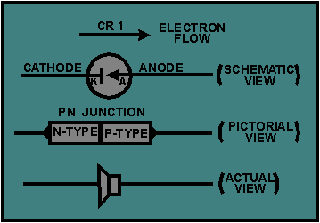
If we join a section of N-type semiconductor material with a similar section of P-type semiconductor material, we obtain a device known as a PN JUNCTION. (The area where the N and P regions meet is appropriately called the junction.) The usual characteristics of this device make it extremely useful in electronics as a diode rectifier. The diode rectifier or PN junction diode performs the same function as its counterpart in electron tubes but in a different way. The diode is nothing more than a two-element semiconductor device that makes use of the rectifying properties of a PN junction to convert alternating current into direct current by permitting current flow in only one direction. The schematic symbol of a PN junction diode is shown in figure 1-12. The vertical bar represents the cathode (N-type material) since it is the source of electrons and the arrow represents the anode. (P-type material) since it is the destination of the electrons. The label "CR1" is an alphanumerical code used to identify the diode. In this figure, we have only one diode so it is labeled CR1 (crystal rectifier number one). If there were four diodes shown in the diagram, the last diode would be labeled CR4. The heavy dark line shows electron flow. Notice it is against the arrow. For further clarification, a pictorial diagram of a PN junction and an actual semiconductor (one of many types) are also illustrated.
Figure 1-12. - The PN junction diode.
CONSTRUCTION
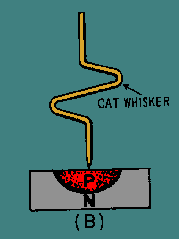
Merely pressing together a section of P material and a section of N material, however, is not sufficient to produce a rectifying junction. The semiconductor should be in one piece to form a proper PN junction, but divided into a P-type impurity region and an N-type impurity region. This can be done in various ways. One way is to mix P-type and N-type impurities into a single crystal during the manufacturing process. By so doing, a P-region is grown over part of a semiconductor's length and N-region is grown over the other part. This is called a GROWN junction and is illustrated in view A of figure 1-13. Another way to produce a PN junction is to melt one type of impurity into a semiconductor of the opposite type impurity. For example, a pellet of acceptor impurity is placed on a wafer of N-type germanium and heated. Under controlled temperature conditions, the acceptor impurity fuses into the wafer to form a P-region within it, as shown in view B of figure 1-13. This type of junction is known as an ALLOY or FUSED-ALLOY junction, and is one of the most commonly used junctions. In figure 1-14, a POINT-CONTACT type of construction is shown. It consists of a fine metal wire, called a cat whisker, that makes contact with a small area on the surface of an N-type semiconductor as shown in view A of the figure. The PN union is formed in this process by momentarily applying a high-surge current to the wire and the N-type semiconductor. The heat generated by this current converts the material nearest the point of contact to a P-type material (view B).
Figure 1-13. - Grown and fused PN junctions from which bars are cut.
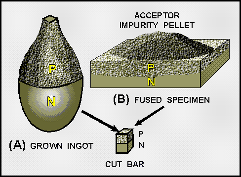
Figure 1-14A. - The point-contact type of diode construction.
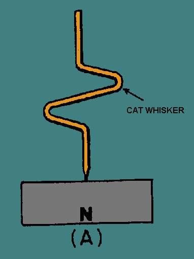
Figure 1-14B. - The point-contact type of diode construction.
Still another process is to heat a section of semiconductor material to near melting and then diffuse impurity atoms into a surface layer. Regardless of the process, the objective is to have a perfect bond everywhere along the union (interface) between P and N materials. Proper contact along the union is important because, as we will see later, the union (junction or interface) is the rectifying agent in the diode.
PN JUNCTION OPERATION
Now that you are familiar with P- and N-type materials, how these materials are joined together to form a diode, and the function of the diode, let us continue our discussion with the operation of the PN junction. But before we can understand how the PN junction works, we must first consider current flow in the materials that make up the junction and what happens initially within the junction when these two materials are joined together.
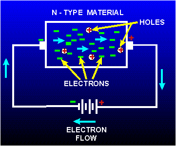
Current Flow in the N-Type Material
Conduction in the N-type semiconductor, or crystal, is similar to conduction in a copper wire. That is, with voltage applied across the material, electrons will move through the crystal just as current would flow in a copper wire. This is shown in figure 1-15. The positive potential of the battery will attract the free electrons in the crystal. These electrons will leave the crystal and flow into the positive terminal of the battery. As an electron leaves the crystal, an electron from the negative terminal of the battery will enter the crystal, thus completing the current path. Therefore, the majority current carriers in the N-type material (electrons) are repelled by the negative side of the battery and move through the crystal toward the positive side of the battery.
Figure 1-15. - Current flow In the N-type material.
Current Flow in the P-Type Material
Current flow through the P-type material is illustrated in figure 1-16. Conduction in the P material is by positive holes, instead of negative electrons. A hole moves from the positive terminal of the P material to the negative terminal. Electrons from the external circuit enter the negative terminal of the material and fill holes in the vicinity of this terminal. At the positive terminal, electrons are removed from the covalent bonds, thus creating new holes. This process continues as the steady stream of holes (hole current) moves toward the negative terminal.
Figure 1-16. - Current flow In the P-type material.
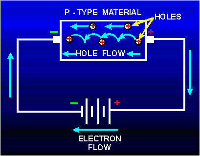
Notice in both N-type and P-type materials, current flow in the external circuit consists of electrons moving out of the negative terminal of the battery and into the positive terminal of the battery. Hole flow, on the other hand, only exists within the material itself.
Junction Barrier
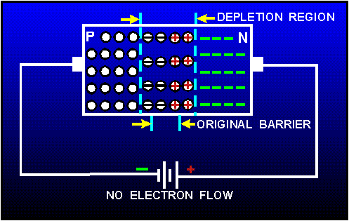
Although the N-type material has an excess of free electrons, it is still electrically neutral. This is because the donor atoms in the N material were left with positive charges after free electrons became available by covalent bonding (the protons outnumbered the electrons). Therefore, for every free electron in the N material, there is a corresponding positively charge atom to balance it. The end result is that the N material has an overall charge of zero.
By the same reasoning, the P-type material is also electrically neutral because the excess of holes in this material is exactly balanced by the number of electrons. Keep in mind that the holes and electrons are still free to move in the material because they are only loosely bound to their parent atoms.
It would seem that if we joined the N and P materials together by one of the processes mentioned earlier, all the holes and electrons would pair up. On the contrary, this does not happen. Instead the electrons in the N material diffuse (move or spread out) across the junction into the P material and fill some of the holes. At the same time, the holes in the P material diffuse across the junction into the N material and are filled by N material electrons. This process, called JUNCTION RECOMBINATION, reduces the number of free electrons and holes in the vicinity of the junction. Because there is a depletion, or lack of free electrons and holes in this area, it is known as the DEPLETION REGION.
The loss of an electron from the N-type material created a positive ion in the N material, while the loss of a hole from the P material created a negative ion in that material. These ions are fixed in place in the crystal lattice structure and cannot move. Thus, they make up a layer of fixed charges on the two sides of the junction as shown in figure 1-17.
On the N side of the junction, there is a layer of positively charged ions; on the P side of the junction, there is a layer of negatively charged ions. An electrostatic field, represented by a small battery in the figure, is established across the junction between the oppositely charged ions. The diffusion of electrons and holes across the junction will continue until the magnitude of the electrostatic field is increased to the point where the electrons and holes no longer have enough energy to overcome it, and are repelled by the negative and positive ions respectively. At this point equilibrium is established and, for all practical purposes, the movement of carriers across the junction ceases. For this reason, the electrostatic field created by the positive and negative ions in the depletion region is called a barrier.
Figure 1-17. - The PN junction barrier formation.
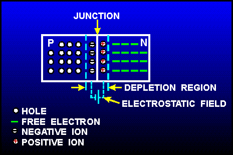
The action just described occurs almost instantly when the junction is formed. Only the carriers in the immediate vicinity of the junction are affected. The carriers throughout the remainder of the N and P material are relatively undisturbed and remain in a balanced condition.
FORWARD BIAS. - An external voltage applied to a PN junction is call BIAS. If, for example, a battery is used to supply bias to a PN junction and is connected so that its voltage opposes the junction field, it will reduce the junction barrier and, therefore, aid current flow through the junction. This type of bias is known as forward bias, and it causes the junction to offer only minimum resistance to the flow of current.
Notice the positive terminal of the bias battery is connected to the P-type material and the negative terminal of the battery is connected to the N-type material. The positive potential repels holes toward the junction where they neutralize some of the negative ions. At the same time the negative potential repels electrons toward the junction where they neutralize some of the positive ions. Since ions on both sides of the barrier are being neutralized, the width of the barrier decreases. Thus, the effect of the battery voltage in the forward-bias direction is to reduce the barrier potential across the junction and to allow majority carriers to cross the junction. Current flow in the forward-biased PN junction is relatively simple. An electron leaves the negative terminal of the battery and moves to the terminal of the N-type material. It enters the N material, where it is the majority carrier and moves to the edge of the junction barrier. Because of forward bias, the barrier offers less opposition to the electron and it will pass through the depletion region into the P-type material. The electron loses energy in overcoming the opposition of the junction barrier, and upon entering the P material, combines with a hole. The hole was produced when an electron was extracted from the P material by the positive potential of the battery. The created hole moves through the P material toward the junction where it combines with an electron.
Figure 1-18. - Forward-biased PN junction.
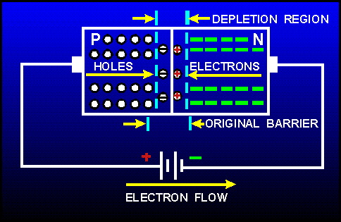
It is important to remember that in the forward biased condition, conduction is by MAJORITY current carriers (holes in the P-type material and electrons in the N-type material). Increasing the battery voltage will increase the number of majority carriers arriving at the junction and will therefore increase the current flow. If the battery voltage is increased to the point where the barrier is greatly reduced, a heavy current will flow and the junction may be damaged from the resulting heat.
REVERSE BIAS. - If the battery mentioned earlier is connected across the junction so that its voltage aids the junction, it will increase the junction barrier and thereby offer a high resistance to the current flow through the junction. This type of bias is known as reverse bias.
To reverse bias a junction diode, the negative battery terminal is connected to the P-type material, and the positive battery terminal to the N-type material as shown in figure 1-19. The negative potential attracts the holes away from the edge of the junction barrier on the P side, while the positive potential attracts the electrons away from the edge of the barrier on the N side. This action increases the barrier width because there are more negative ions on the P side of the junction, and more positive ions on the N side of the junction. Notice in the figure the width of the barrier has increased. This increase in the number of ions prevents current flow across the junction by majority carriers. However, the current flow across the barrier is not quite zero because of the minority carriers crossing the junction. As you recall, when the crystal is subjected to an external source of energy (light, heat, etc.), electron-hole pairs are generated. The electron-hole pairs produce minority current carriers. There are minority current carriers in both regions: holes in the N material and electrons in the P material. With reverse bias, the electrons in the P-type material are repelled toward the junction by the negative terminal of the battery. As the electron moves across the junction, it will neutralize a positive ion in the N-type material. Similarly, the holes in the N-type material will be repelled by the positive terminal of the battery toward the junction. As the hole crosses the junction, it will neutralize a negative ion in the P-type material. This movement of minority carriers is called MINORITY CURRENT FLOW, because the holes and electrons involved come from the electron-hole pairs that are generated in the crystal lattice structure, and not from the addition of impurity atoms.
Figure 1-19. - Reverse-biased PN junction.
Therefore, when a PN junction is reverse biased, there will be no current flow because of majority carriers but a very small amount of current because of minority carriers crossing the junction. However, at normal operating temperatures, this small current may be neglected.
In summary, the most important point to remember about the PN junction diode is its ability to offer very little resistance to current flow in the forward-bias direction but maximum resistance to current flow when reverse biased. A good way of illustrating this point is by plotting a graph of the applied voltage versus the measured current. Figure 1-20 shows a plot of this voltage-current relationship (characteristic curve) for a typical PN junction diode.
Figure 1-20. - PN junction diode characteristic curve.
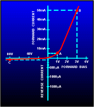
To determine the resistance from the curve in this figure we can use Ohm's law:

For example at point A the forward-bias voltage is 1 volt and the forward-bias current is 5 milliamperes. This represents 200 ohms of resistance (1 volt/5mA = 200 ohms). However, at point B the voltage is 3 volts and the current is 50 milliamperes. This results in 60 ohms of resistance for the diode. Notice that when the forward-bias voltage was tripled (1 volt to 3 volts), the current increased 10 times (5mA to 50 mA). At the same time the forward-bias voltage increased, the resistance decreased from 200 ohms to 60 ohms. In other words, when forward bias increases, the junction barrier gets smaller and its resistance to current flow decreases.
On the other hand, the diode conducts very little when reverse biased. Notice at point C the reverse bias voltage is 80 volts and the current is only 100 microamperes. This results in 800 k ohms of resistance, which is considerably larger than the resistance of the junction with forward bias. Because of these unusual features, the PN junction diode is often used to convert alternating current into direct current (rectification).
PN JUNCTION APPLICATION
Until now, we have mentioned only one application for the diode-rectification, but there are many more applications that we have not yet discussed. Variations in doping agents, semiconductor materials, and manufacturing techniques have made it possible to produce diodes that can be used in many different applications. Examples of these types of diodes are signal diodes, rectifying diodes, Zener diodes (voltage protection diodes for power supplies), varactors (amplifying and switching diodes), and many more. Only applications for two of the most commonly used diodes, the signal diode and rectifier diode, will be presented in this chapter. The other diodes will be explained later on in this module.
Half-Wave Rectifier
One of the most important uses of a diode is rectification. The normal PN junction diode is well-suited for this purpose as it conducts very heavily when forward biased (low-resistance direction) and only slightly when reverse biased (high-resistance direction). If we place this diode in series with a source of ac power, the diode will be forward and reverse biased every cycle. Since in this situation current flows more easily in one direction than the other, rectification is accomplished. The simplest rectifier circuit is a half-wave rectifier (fig. 1-21 view A and view B) which consists of a diode, an ac power source, and a load resister.
Figure 1-21A. - Simple half-wave rectifier.
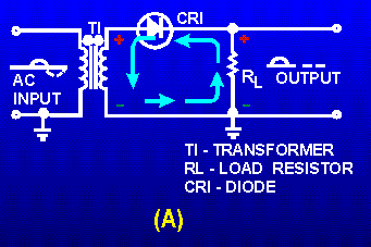
Figure 1-21B. - Simple half-wave rectifier.
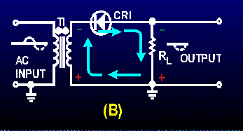
The transformer (T1) in the figure provides the ac input to the circuit; the diode (CR1) provides the rectification; and the load resistor (RL) serves two purposes: it limits the amount of current flow in the circuit to a safe level, and it also develops the output signal because of the current flow through it.
Before describing how this circuit operates, the definition of the word "load" as it applies to power supplies must be understood. Load is defined as any device that draws current. A device that draws little current is considered a light load, whereas a device that draws a large amount of current is a heavy load. Remember that when we speak of "load," we are speaking about the device that draws current from the power source. This device may be a simple resistor, or one or more complicated electronic circuits.
During the positive half-cycle of the input signal (solid line) in figure 1-21 view A, the top of the transformer is positive with respect to ground. The dots on the transformer indicate points of the same polarity. With this condition the diode is forward biased, the depletion region is narrow, the resistance of the diode is low, and current flows through the circuit in the direction of the solid lines. When this current flows through the load resistor, it develops a negative to positive voltage drop across it, which appears as a positive voltage at the output terminal.
When the ac input goes in a negative direction (fig. 1-21 view A), the top of the transformer becomes negative and the diode becomes reverse biased. With reverse bias applied to the diode, the depletion region increases, the resistance of the diode is high, and minimum current flows through the diode. For all practical purposes, there is no output developed across the load resistor during the negative alternation of the input signal as indicated by the broken lines in the figure. Although only one cycle of input is shown, it should be realized that the action described above continually repeats itself, as long as there is an input. Therefore, since only the positive half-cycles appear at the output this circuit converted the ac input into a positive pulsating dc voltage. The frequency of the output voltage is equal to the frequency of the applied ac signal since there is one pulse out for each cycle of the ac input. For example, if the input frequency is 60 hertz (60 cycles per second), the output frequency is 60 pulses per second (pps).
However, if the diode is reversed as shown in view B of figure 1-21, a negative output voltage would be obtained. This is because the current would be flowing from the top of RL toward the bottom, making the output at the top of RL negative with respect to the bottom or ground. Because current flows in this circuit only during half of the input cycle, it is called a half-wave rectifier.
The semiconductor diode shown in the figure can be replaced by a metallic rectifier and still achieve the same results. The metallic rectifier, sometimes referred to as a dry-disc rectifier, is a metal-to-semiconductor, large-area contact device. Its construction is distinctive; a semiconductor is sandwiched between two metal plates, or electrodes, as shown in figure 1-22.
Note in the figure that a barrier, with a resistance many times greater than that of the semiconductor material, is constructed on one of the metal electrodes. The contact having the barrier is a rectifying contact; the other contact is nonrectifying. Metallic rectifiers act just like the diodes previously discussed in that they permit current to flow more readily in one direction than the other. However, the metallic rectifier is fairly large compared to the crystal diode as can be seen in figure 1-23. The reason for this is: metallic rectifier units are stacked (to prevent inverse voltage breakdown), have large area plates (to handle high currents), and usually have cooling fins (to prevent overheating).
Figure 1-22. - A metallic rectifier.
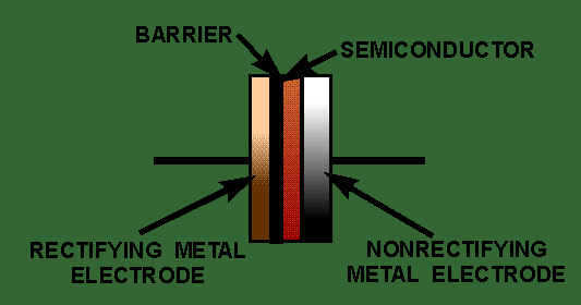
Figure 1-23. - Different types of crystal and metallic rectifiers.
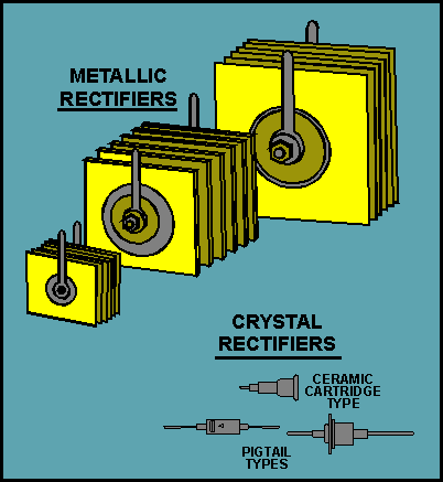
There are many known metal-semiconductor combinations that can be used for contact rectification. Copper oxide and selenium devices are by far the most popular. Copper oxide and selenium are frequently used over other types of metallic rectifiers because they have a large forward current per unit contact area, low forward voltage drop, good stability, and a lower aging rate. In practical application, the selenium rectifier is used where a relatively large amount of power is required. On the other hand, copper-oxide rectifiers are generally used in small-current applications such as ac meter movements or for delivering direct current to circuits requiring not more than 10 amperes.
Since metallic rectifiers are affected by temperature, atmospheric conditions, and aging (in the case of copper oxide and selenium), they are being replaced by the improved silicon crystal rectifier. The silicon rectifier replaces the bulky selenium rectifier as to current and voltage rating, and can operate at higher ambient (surrounding) temperatures.
Diode Switch
In addition to their use as simple rectifiers, diodes are also used in circuits that mix signals together (mixers), detect the presence of a signal (detector), and act as a switch "to open or close a circuit." Diodes used in these applications are commonly referred to as "signal diodes." The simplest application of a signal diode is the basic diode switch shown in figure 1-24.
Figure 1-24. - Basic diode switch.
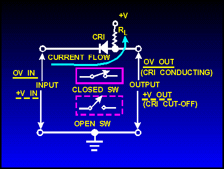
When the input to this circuit is at zero potential, the diode is forward biased because of the zero potential on the cathode and the positive voltage on the anode. In this condition, the diode conducts and acts as a straight piece of wire because of its very low forward resistance. In effect, the input is directly coupled to the output resulting in zero volts across the output terminals. Therefore, the diode, acts as a closed switch when its anode is positive with respect to its cathode.
If we apply a positive input voltage (equal to or greater than the positive voltage supplied to the anode) to the diode's cathode, the diode will be reverse biased. In this situation, the diode is cut off and acts as an open switch between the input and output terminals. Consequently, with no current flow in the circuit, the positive voltage on the diode's anode will be felt at the output terminal. Therefore, the diode acts as an open switch when it is reverse biased.
DIODE CHARACTERISTICS
Semiconductor diodes have properties that enable them to perform many different electronic functions. To do their jobs, engineers and technicians must be supplied with data on these different types of diodes. The information presented for this purpose is called DIODE CHARACTERISTICS. These characteristics are supplied by manufacturers either in their manuals or on specification sheets (data sheets). Because of the scores of manufacturers and numerous diode types, it is not practical to put before you a specification sheet and call it typical. Aside from the difference between manufacturers, a single manufacturer may even supply specification sheets that differ both in format and content. Despite these differences, certain performance and design information is normally required. We will discuss this information in the next few paragraphs.
A standard specification sheet usually has a brief description of the diode. Included in this description is the type of diode, the major area of application, and any special features. Of particular interest is the specific application for which the diode is suited. The manufacturer also provides a drawing of the diode which gives dimension, weight, and, if appropriate, any identification marks. In addition to the above data, the following information is also provided: a static operating table (giving spot values of parameters under fixed conditions), sometimes a characteristic curve similar to the one in figure 1-20 (showing how parameters vary over the full operating range), and diode ratings (which are the limiting values of operating conditions outside which could cause diode damage).
Manufacturers specify these various diode operating parameters and characteristics with "letter symbols" in accordance with fixed definitions. The following is a list, by letter symbol, of the major electrical characteristics for the rectifier and signal diodes.
RECTIFIER DIODES
DC BLOCKING VOLTAGE [VR] - the maximum reverse dc voltage that will not cause breakdown.
AVERAGE FORWARD VOLTAGE DROP [VF(AV)] - the average forward voltage drop across the rectifier given at a specified forward current and temperature.
AVERAGE RECTIFIER FORWARD CURRENT [IF(AV)] - the average rectified forward current at a specified temperature, usually at 60 Hz with a resistive load.
AVERAGE REVERSE CURRENT [IR(AV)] - the average reverse current at a specified temperature, usually at 60 Hz.
PEAK SURGE CURRENT [ISURGE] - the peak current specified for a given number of cycles or portion of a cycle.
SIGNAL DIODES
PEAK REVERSE VOLTAGE [PRV] - the maximum reverse voltage that can be applied before reaching the breakdown point. (PRV also applies to the rectifier diode.)
REVERSE CURRENT [IR] - the small value of direct current that flows when a semiconductor diode has reverse bias
MAXIMUM FORWARD VOLTAGE DROP AT INDICATED FORWARD CURRENT [VF@IF] - the maximum forward voltage drop across the diode at the indicated forward current.
REVERSE RECOVERY TIME [trr] - the maximum time taken for the forward-bias diode to recover its reverse bias.
The ratings of a diode (as stated earlier) are the limiting values of operating conditions, which if exceeded could cause damage to a diode by either voltage breakdown or overheating. The PN junction diodes are generally rated for: MAXIMUM AVERAGE FORWARD CURRENT, PEAK RECURRENT FORWARD CURRENT, MAXIMUM SURGE CURRENT, and PEAK REVERSE VOLTAGE.
Maximum average forward current is usually given at a special temperature, usually 25°C, (77°F) and refers to the maximum amount of average current that can be permitted to flow in the forward direction. If this rating is exceeded, structure breakdown can occur.
Peak recurrent forward current is the maximum peak current that can be permitted to flow in the forward direction in the form of recurring pulses.
Maximum surge current is the maximum current permitted to flow in the forward direction in the form of nonrecurring pulses. Current should not equal this value for more than a few milliseconds.
Peak reverse voltage (PRV) is one of the most important ratings. PRV indicates the maximum reverse-bias voltage that may be applied to a diode without causing junction breakdown.
All of the above ratings are subject to change with temperature variations. If, for example, the operating temperature is above that stated for the ratings, the ratings must be decreased.
DIODE IDENTIFICATION
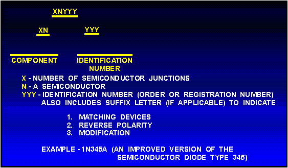
There are many types of diodes varying in size from the size of a pinhead (used in subminiature circuitry) to large 250-ampere diodes (used in high-power circuits). Because there are so many different types of diodes, some system of identification is needed to distinguish one diode from another. This is accomplished with the semiconductor identification system shown in figure 1-25. This system is not only used for diodes but transistors and many other special semiconductor devices as well. As illustrated in this figure, the system uses numbers and letters to identify different types of semiconductor devices. The first number in the system indicates the number of junctions in the semiconductor device and is a number, one less than the number of active elements. Thus 1 designates a diode; 2 designates a transistor (which may be considered as made up of two diodes); and 3 designates a tetrode (a four-element transistor). The letter "N" following the first number indicates a semiconductor. The 2- or 3-digit number following the letter "N" is a serialized identification number. If needed, this number may contain a suffix letter after the last digit. For example, the suffix letter "M" may be used to describe matching pairs of separate semiconductor devices or the letter "R" may be used to indicate reverse polarity. Other letters are used to indicate modified versions of the device which can be substituted for the basic numbered unit. For example, a semiconductor diode designated as type 1N345A signifies a two-element diode (1) of semiconductor material (N) that is an improved version (A) of type 345.
Figure 1-25. - Semiconductor identification codes.
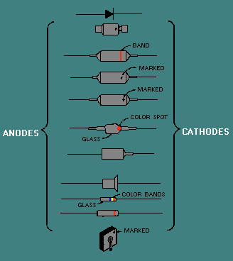
When working with these different types of diodes, it is also necessary to distinguish one end of the diode from the other (anode from cathode). For this reason, manufacturers generally code the cathode end of the diode with a "k," "+," "cath," a color dot or band, or by an unusual shape (raised edge or taper) as shown in figure 1-26. In some cases, standard color code bands are placed on the cathode end of the diode. This serves two purposes: (1) it identifies the cathode end of the diode, and (2) it also serves to identify the diode by number.
Figure 1-26. - Semiconductor diode markings.
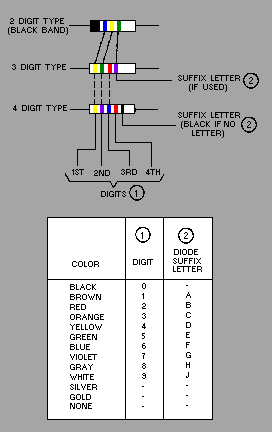
The standard diode color code system is shown in figure 1-27. Take, for example, a diode with brown, orange, and white bands at one terminal and figure out its identification number. With brown being a "1," orange a "3," and white "9," the device would be identified as a type 139 semiconductor diode, or specifically 1N139.
Figure 1-27. - Semiconductor diode color code system.
Keep in mind, whether the diode is a small crystal type or a large power rectifier type, both are still represented schematically, as explained earlier, by the schematic symbol shown in figure 1-12.
Freddy R Vallenilla R
16.791.006
EES SEC 2
No hay comentarios:
Publicar un comentario