domingo, 25 de julio de 2010

Nanowires Key to Future Transistors


A new generation of ultrasmall transistors and more powerful computer chips using tiny structures called semiconducting nanowires are closer to reality after a key discovery by researchers at IBM, Purdue University and the University of California at Los Angeles.


Researchers are closer to using tiny devices called semiconducting nanowires to create a new generation of ultrasmall transistors and more powerful computer chips. The researchers have grown the nanowires with sharply defined layers of silicon and germanium, offering better transistor performance. As depicted in this illustration, tiny particles of a gold-aluminum alloy were alternately heated and cooled inside a vacuum chamber, and then silicon and germanium gases were alternately introduced. As the gold-aluminum bead absorbed the gases, it became "supersaturated" with silicon and germanium, causing them to precipitate and form wires. (Credit: Purdue University, Birck Nanotechnology Center/Seyet LLC)

The researchers have learned how to create nanowires with layers of different materials that are sharply defined at the atomic level, which is a critical requirement for making efficient transistors out of the structures.

"Having sharply defined layers of materials enables you to improve and control the flow of electrons and to switch this flow on and off," said Eric Stach, an associate professor of materials engineering at Purdue.

Electronic devices are often made of "heterostructures," meaning they contain sharply defined layers of different semiconducting materials, such as silicon and germanium. Until now, however, researchers have been unable to produce nanowires with sharply defined silicon and germanium layers. Instead, this transition from one layer to the next has been too gradual for the devices to perform optimally as transistors.

The new findings point to a method for creating nanowire transistors.

The findings are detailed in a research paper appearing Nov. 27 in the journal Science. The paper was written by Purdue postdoctoral researcher Cheng-Yen Wen, Stach, IBM materials scientists Frances Ross, Jerry Tersoff and Mark Reuter at the Thomas J. Watson Research Center in Yorktown Heights, N.Y, and Suneel Kodambaka, an assistant professor at UCLA's Department of Materials Science and Engineering.

Whereas conventional transistors are made on flat, horizontal pieces of silicon, the silicon nanowires are "grown" vertically. Because of this vertical structure, they have a smaller footprint, which could make it possible to fit more transistors on an integrated circuit, or chip, Stach said.

"But first we need to learn how to manufacture nanowires to exacting standards before industry can start using them to produce transistors," he said.

Nanowires might enable engineers to solve a problem threatening to derail the electronics industry. New technologies will be needed for industry to maintain Moore's law, an unofficial rule stating that the number of transistors on a computer chip doubles about every 18 months, resulting in rapid progress in computers and telecommunications. 

Doubling the number of devices that can fit on a computer chip translates into a similar increase in performance. However, it is becoming increasingly difficult to continue shrinking electronic devices made of conventional silicon-based semiconductors.

"In something like five to, at most, 10 years, silicon transistor dimensions will have been scaled to their limit," Stach said.
Transistors made of nanowires represent one potential way to continue the tradition of Moore's law.

The researchers used an instrument called a transmission electron microscope to observe the nanowire formation. Tiny particles of a gold-aluminum alloy were first heated and melted inside a vacuum chamber, and then silicon gas was introduced into the chamber. As the melted gold-aluminum bead absorbed the silicon, it became "supersaturated" with silicon, causing the silicon to precipitate and form wires. Each growing wire was topped with a liquid bead of gold-aluminum so that the structure resembled a mushroom.

Then, the researchers reduced the temperature inside the chamber enough to cause the gold-aluminum cap to solidify, allowing germanium to be deposited onto the silicon precisely and making it possible to create a heterostructure of silicon and germanium.

The cycle could be repeated, switching the gases from germanium to silicon as desired to make specific types of heterostructures, Stach said.

Having a heterostructure makes it possible to create a germanium "gate" in each transistor, which enables devices to switch on and off.

The work is based at IBM's Thomas J. Watson Research Center and Purdue's Birck Nanotechnology Center in the university's Discovery Park and is funded by the National Science Foundation through the NSF's Electronic and Photonic Materials Program in the Division of Materials Research.

Freddy Vallenilla, EES SECC 2

New 'FinFETs' Promising For Smaller Transistors, More Powerful Chips


Purdue University researchers are making progress in developing a new type of transistor that uses a finlike structure instead of the conventional flat design, possibly enabling engineers to create faster and more compact circuits and computer chips.

Researchers are making progress in developing new types of transistors, called finFETs, which use a finlike structure instead of the conventional flat design, possibly enabling engineers to create faster and more compact circuits and computer chips. The fins are made not of silicon, but from a material called indium-gallium-arsenide, as shown in this illustration. (Credit: Birck Nanotechnology Center, Purdue University)

The fins are made not of silicon, like conventional transistors, but from a material called indium-gallium-arsenide. Called finFETs, for fin field-effect-transistors, researchers from around the world have been working to perfect the devices as potential replacements for conventional transistors.

In work led by Peide Ye, an associate professor of electrical and computer engineering, the Purdue researchers are the first to create finFETs using a technology called atomic layer deposition. Because atomic layer deposition is commonly used in industry, the new finFET technique may represent a practical solution to the coming limits of conventional silicon transistors.

"We have just demonstrated the proof of concept here," Ye said.

Findings are detailed in three research papers being presented during the International Electron Devices Meeting on Dec. 7-9 in Baltimore. The work is led by doctoral student Yanqing Wu, who provided major contributions for two of the papers.

The finFETs might enable engineers to sidestep a problem threatening to derail the electronics industry. New technologies will be needed for industry to keep pace with Moore's law, an unofficial rule stating that the number of transistors on a computer chip doubles about every 18 months, resulting in rapid progress in computers and telecommunications. Doubling the number of devices that can fit on a computer chip translates into a similar increase in performance. However, it is becoming increasingly difficult to continue shrinking electronic devices made of conventional silicon-based semiconductors.

In addition to making smaller transistors possible, finFETs also might conduct electrons at least five times faster than conventional silicon transistors, called MOSFETs, or metal-oxide-semiconductor field-effect transistors.

"The potential increase in speed is very important," Ye said. "The finFETs could enable industry to not only create smaller devices, but also much faster computer processors."
Transistors contain critical components called gates, which enable the devices to switch on and off and to direct the flow of electrical current. In today's chips, the length of these gates is about 45 nanometers, or billionths of a meter.

The semiconductor industry plans to reduce the gate length to 22 nanometers by 2015. However, further size reductions and boosts in speed are likely not possible using silicon, meaning new designs and materials will be needed to continue progress.

Indium-gallium-arsenide is among several promising semiconductor alloys being studied to replace silicon. Such alloys are called III-V materials because they combine elements from the third and fifth groups of the periodical table.

Creating smaller transistors also will require finding a new type of insulating layer essential for the devices to switch off. As gate lengths are made smaller than 22 nanometers, the silicon dioxide insulator used in conventional transistors fails to perform properly and is said to "leak" electrical charge.

One potential solution to this leaking problem is to replace silicon dioxide with materials that have a higher insulating value, or "dielectric constant," such as hafnium dioxide or aluminum oxide.

The Purdue research team has done so, creating finFETs that incorporate the indium-gallium-arsenide fin with a so-called "high-k" insulator. Previous attempts to use indium-gallium-arsenide finFETs to make devices have failed because too much current leaks from the circuit.

The researchers are the first to "grow" hafnium dioxide onto finFETs made of a III-V material using atomic layer deposition. The approach could make it possible to create transistors using the thinnest insulating layers possible -- only a single atomic layer thick.

The finlike design is critical to preventing current leakage, in part because the vertical structure can be surrounded by an insulator, whereas a flat device has the insulator on one side only.

The work is funded by the National Science Foundation and the Semiconductor Research Consortium and is based at the Birck Nanotechnology Center in Purdue's Discovery Park.


Freddy Vallenilla, EES SECC 2

Breakthrough in 'Spintronics' Could Lead to Energy Efficient Chips


Scientists from the MESA Institute for Nanotechnology of the University of Twente and the FOM Foundation have succeeded in transferring magnetic information directly into a semiconductor. For the first time, this is achieved at room temperature. This breakthrough brings the development of a more energy efficient form of electronics, so-called 'spintronics' within reach.

Silicon spin sandwich. (Credit: Image courtesy of University of Twente)

So far, information exchange between a magnetic material and a semiconductor was only possible at very low temperature. The successful demonstration of information exchange at room temperature is a pivotal step in the development of an alternative paradigm for electronics. The main advantage of this new 'spintronics' technology is the reduced power consumption: in present-day computer chips, excessive heat production is already a problem, and this will soon become a limiting factor.

Digital by nature
Unlike conventional electronics that employs the charge of the electron and its transport, spintronics exploits another important property of the electron, namely the 'spin'. The sense of rotation of an electron is represented by a spin that either points up or down. In magnetic materials, the spin orientation can be used to store a bit of information as a '1' or a '0'. The challenge is to transfer this spin information to a semiconductor, such that the information can be processed in new spin-based electronic components. These are expected to operate at lower power consumption, since computations such as reversing the electron spin, require less power than the usual transport of charge.

Only a few atomic layers thick
To achieve an efficient information exchange, the researchers insert an ultra thin -- less than one nanometer thick -- layer of aluminum oxide between the magnetic material and the semiconductor: this corresponds to only a few atomic layers. The thickness and quality of this layer are crucial. The information is transferred by applying an electric current across the oxide interface, thereby introducing a magnetization in the semiconductor, with a controllable magnitude and orientation.
Importantly, the method works for silicon: the prevalent electronic material for which highly advanced fabrication technology is available. The researchers found that the spin information can propagate into the silicon to a depth of several hundred nanometers. This is sufficient for the operation of nanoscale spintronic components, according to researcher Ron Jansen. Now the next step is: to built new electronic components and circuits and use these to manipulate spin information.
The spintronics research is performed by a team of researchers led by Ron Jansen at the MESA+ Institute for Nanotechnology, and is made possible by financial support from the Foundation FOM and a VIDI-grant received from the Netherlands Organization for Scientific Research (NWO).

Freddy Vallenilla, EES SECC 2

sábado, 24 de julio de 2010

High electron mobility transistor


High electron mobility transistor (HEMT), also known as heterostructure FET (HFET) or modulation-doped FET (MODFET), is a field effect transistor incorporating a junction between two materials with different band gaps as the channel instead of a doped region, as is generally the case for MOSFET. A commonly used material combination is GaAs with AlGaAs, though there is wide variation, dependent on the application of the device. Devices incorporating more indium generally show better high-frequency performance, while in recent years, gallium nitride HEMTs have attracted attention due to their high-power performance.

Cross section of a GaAs/AlGaAs/InGaAs pHEMT

To allow conduction, semiconductors are doped with impurities which donate mobile electrons (or holes). However, these electrons are slowed down through collisions with the impurities (dopants) used to generate them in the first place. HEMTs avoid this through the use of high mobility electrons generated using the heterojunction of a highly-doped wide-bandgap n-type donor-supply layer (AlGaAs in our example) and a non-doped narrow-bandgap channel layer with no dopant impurities (GaAs in this case).

The electrons generated in the thin n-type AlGaAs layer drop completely into the GaAs layer to form a depleted AlGaAs layer, because the heterojunction created by different band-gap materials forms a quantum well (a steep canyon) in the conduction band on the GaAs side where the electrons can move quickly without colliding with any impurities because the GaAs layer is undoped, and from which they cannot escape. The effect of this is to create a very thin layer of highly mobile conducting electrons with very high concentration, giving the channel very low resistivity (or to put it another way, "high electron mobility"). This layer is called a two-dimensional electron gas. As with all the other types of FETs, a voltage applied to the gate alters the conductivity of this layer.

Ordinarily, the two different materials used for a heterojunction must have the same lattice constant (spacing between the atoms). As an analogy, imagine pushing together two plastic combs with a slightly different spacing. At regular intervals, you'll see two teeth clump together. In semiconductors, these discontinuities form deep-level traps, and greatly reduce device performance.

Band structure in GaAs/AlGaAs heterojunction based HEMT

A HEMT where this rule is violated is called a pHEMT or pseudomorphic HEMT. This is achieved by using an extremely thin layer of one of the materials – so thin that the crystal lattice simply stretches to fit the other material. This technique allows the construction of transistors with larger bandgap differences than otherwise possible, giving them better performance.

Another way to use materials of different lattice constants is to place a buffer layer between them. This is done in the mHEMT or metamorphic HEMT, an advancement of the pHEMT. The buffer layer is made of AlInAs, with the indium concentration graded so that it can match the lattice constant of both the GaAs substrate and the GaInAs channel. This brings the advantage that practically any Indium concentration in the channel can be realized, so the devices can be optimized for different applications (low indium concentration provides low noise; high indium concentration gives high gain).

Applications are similar to those of MESFETs – microwave and millimeter wave communications, imaging, radar, and radio astronomy – any application where high gain and low noise at high frequencies are required. HEMTs have shown current gain to frequencies greater than 600 GHz and power gain to frequencies greater than 1 THz. (Heterojunction bipolar transistors were demonstrated at current gain frequencies over 600 GHz in April 2005.) Numerous companies worldwide develop and manufacture HEMT-based devices. These can be discrete transistors but are more usually in the form of a 'monolithic microwave integrated circuit' (MMIC). HEMTs are found in many types of equipment ranging from cellphones and DBS receivers to electronic warfare systems such as radar and for radio astronomy.

The invention of the HEMT is usually attributed to Takashi Mimura (三村 高志) (Fujitsu, Japan). However, Ray Dingle and his co-workers in Bell Laboratories also played an important role in the invention of the HEMT.


Freddy Vallenilla, EES SECC 2

InP/GaInAs Single and Double Heterostructure Bipolar Transistors


InP/GaInAs HBTs are of central importance to the development of modern lightwave communication systems such as 40 Gb/s optical communication systems because they are compatible for integration with 1.3-1.5µm optoelectronic components such as lasers and photodetectors. At present only a few companies like Hughes, TRW, and Lucent provide commercial products based on InP HBTs. InP/GaInAs HBTs are the fastest bipolar transistors ever fabricated, but they present a number of complications related to the low breakdown voltages achievable in the narrow bandgap GaInAs (0.75eV) collectors. Double heterostructure HBTs with a wide bandgap InP or InAlAs collector permit marked improvements in breakdown voltages but tend to cause a blocking effect of electrons flowing through the base and into the collector. The blocking effects can be alleviated by grading the collector/base junction alloy composition, and various schemes have been developed (binary or chirped superlattice grading; or analog compositional grading) but all are sensitive to the exact details of the grading scheme.


The figure on the right shows the equilibrium energy band diagram for an abrupt junction double heterostructure InP/GaInAs bipolar transistor. Complex grading schemes are required to alleviate the collector current blocking effect.


We MWF also investigating InP/GaInAs DHBTs with an InP collector because InP displays higher peak and saturated electron drift velocities, a high breakdown field of ~480 MV/cm, and a high thermal conductivity which allows an efficient heat dissipation in power HBTs operated at high voltages. 
A fully self-aligned wet etch process was developed with evaporated (rather than electroplated) airbridge interconnects. Relatively large area emitter devices (4x12 µm2) have resulted in current gain cutoff frequencies as high as fT=105GHz with a maximum oscillation frequency fmax=85GHz. Scaling of the emitter width to 1µm will result in fmax values beyond 200GHz.
Figure on the left shown a Scanning Electron Microscope image of a 100GHz fully self-aligned InP/GaInAs heterostructure bipolar transistor with a 750Å base and a 7000Å collector. The emitter is on top. Note the evaporated airbridge interconnects. The process is carried out with wet etches only: the resulting surfaces are damage-free, and large BVceo voltages of 11-12V are achieved.

InP/GaAsSb/InP Double Heterostructure Bipolar Transistors

We have developed InP/GaAsSb/InP DHBTs that overcome the collector blocking effect described above by engineering MOCVD-grown DHBTs in which the GaAsSb p-base conduction band edge sits above the InP conduction band edge: instead of being slowed down by a blocking/opposing field due a to a chemical potential gradient, electrons reaching the base/collector junction benefit from a ballistic injection launching ramp that injects them into the InP collector with a high velocity: it is the total integrated velocity across the collector layer that determines the collector transit time, and we believe the ballistic launcher will prove very helpful in the realization of high speed InP based DHBTs. Our first public report of InP/GaAsSb/InP DHBTs was given at the 1998 IEEE Device Research Conference held June 22-24, 1998 in Charlottesville, VA.


The figure on the upper right shows the equilibrium energy band diagram for an abrupt junction double heterostructure InP/GaAsSb/InP bipolar transistors. Note the ballistic electron launcher at the abrupt base-collector junction. The conduction band discontinuity at the InP/GaAsSb interface was determined by sophisticated high-resolution FTIR photoluminescence measurements of the type II recombination at the interface. The conduction band offset is equal to 0.18eV.


The figure on the left  shows room temperature I-V characteristics for a small area InP/GaAsSb/InP DHBTs. BVceo = 6-8V for a 1500Å InP collector layer. The knee voltage is smaller than 0.2V, a great advantage over the usual 0.6V of conventional GaAs MESFETs/HEMTs and HBTs. The collector offset voltage is 12-15mV because of the complete symmetry of the E/B and B/C heterojunctions.
InP/GaAsSb DHBTs have previously been explored by two other groups (Bellcore / Rockwell), but SFU was the first to demonstrate very nearly ideal Gummel characteristics and record collector Vce offset voltages as low as (12-15mV). The base and collector current ideality factors nb and nc are equal to 1.0 in both normal and reverse operation. Cutoff frequencies as high as 75GHz were also achieved in non-optimized structures. We attribute the improved performance of our devices to the careful selection of the growth conditions by cross-correlating the results of AFM, XRD, FTIR-PL, and device measurements.

Such low offset voltages are very attractive for wireless communication systems because there is an urgent need to develop highly efficient low-voltage power amplifiers: in 1998, wireless handset systems have begun a transition to 3.6V supply voltages (with either a 3-cell NiCd or NiMH or a single cell Li+ battery configuration). Note that in the early 1990's the supply voltage for wireless phones was 7.2V (achieved with 6 NiCd cells)-- so many batteries made the handsets bulky and heavy, and the high power dissipation affected the component lifetime. The drive to low-voltage and high amplifier efficiencies is of course fueled by the consumer demand for small handyphones with long talk-times between recharge cycles. As a 3.6V battery pack discharges, its voltage can drop as low as 2.7-3.0V: the power amplifier must continue to perform well as the supply voltage drops toward its end voltage (when the battery is completely discharged). 
The potential advantages of InP-based HBTs, and particularly those of InP/GaAsSb DHBTs, for wireless handset applications are made very clear by comparing the collector current turn-on characteristics of bipolar transistors for various material systems.


The figure on the right shows measured collector current densities in A/cm2 as a function of Vbe for InP/GaAsSb, InP/GaInAs, Si, and GaInP/GaAs transistors. Note how the voltage required for a certain collector current is much smaller in InP-based HBTs than for GaAs HBTs: this is largely a consequence of the smaller base material energy gaps. Base energy gaps: GaAs=1.42eV; Si=1.12eV; GaInAs=0.75eV; and GaAsSb=0.72eV. The saturation at high currents is due to probe and contact series resistance effects.


Freddy Vallenilla, EES SECC 2

Wide Band Gap Devices in Power Systems


Silicon carbide (SiC) is a wide band gap semiconductor material which is ideal for the production of power switching devices. It has excellent power handling and high-temperature operation capabilities. The defense industry has long been interested in the use of SiC technology for its high power applications, such as electric ships, high power weapon systems, hybrid electric vehicles, and More Electric Aircrafts (MEAs). Power electronics converter systems with SiC-based power semiconductor switching devices are lighter, more compact, and more efficient, making them ideal for high-voltage power electronic applications.

These highly desirable device improvements would also substantially trim the amount of undesirable power losses in electric motor drive power conversion applications. For example, SiC high-temperature electronic sensors and controls on an automobile engine will lead to better combustion monitoring and control, which would result in cleaner burning, more fuel efficient cars. SiC MOSFETs, Schottky diodes or PIN diodes, IGBT, Cascode modules, and JFETs are among the choices of the technologies, depending on maturity levels.


The U.S. Navy's DD(X) next generation destroyer requires power control, distribution, and Integrated Power System (IPS) power conversion at multi-MW levels. The power conversion modules (PCMs) for use in the Integrated Fight Through Power (IFTP) of the IPS would benefit substantially from SiC technology. PCM-1 contains DC-to-DC converters with a required rating of at least 750kW. The transfer switch cabinet has a 5000 amp capacity rated DC switch with 1000VDC. The Ship Service Conversion Modules (SSCMs) in PCM-1 convert the DC input (1000VDC) to a lower DC voltage output (800VDC). Si IGBT modules with a 100KW power rating are currently in use. PCM-2 contains DC-AC inverters (Ship Service Invert Modules/SSIMs) with a required rating of at least of 500kW. PCM-4 consists of the hardware and software necessary to convert AC, three-phase, three-wire (the source neutral is grounded via high impedance at the source), 60Hz power from the propulsion bus to DC power. A PCM-4 consists of a transformer and rectifier to convert 4160VAC (3-phase, 60Hz) to 1000VDC.

The development of More Electric Aircraft (MEA) begins by addressing the need for generation and control of significantly increased on-board aircraft electric power. The present distributed controls and actuators for MEA flight control systems and surfaces are typically electrically-controlled but hydraulically-powered. Future systems should be controlled optically and powered electrically. Devices for generation and protection (circuit breakers) will range from 600 to 1000V and will require reliable devices at current levels up to 1000A. One of the key design requirements for new power generation will be the ability to provide high quality power generation at variable generator frequencies.

Replacement of constant frequency generators having variable frequency capability will eliminate the need for integrated drive subsystems (currently used to cancel out engine speed variations while providing constant generator speeds). Operability in the 300-400°C range with continuous operation will be required. Enabling technologies are: high quality power generation, optical control (optical bi-polar transistors), and smart actuator controls operating at higher voltages, to eliminate the cost and added weight of power conditioners. Since control will generally be provided by short, high-current pulses, the control devices will require both high voltages and high currents (though not as high as power generation and control). Typical ranges are from 600-1000 volts and from 5 to more than 600 amps. SiC diodes and transistors provide the primary enabling technology. The desired device types are SiC MOSFETs, with baseline comparison devices being Si IGBTs, which have been demonstrated above 1 kA current levels. Switch mode power conversion transistors are considered better than thyristors for these applications.

Solid-state systems, including flexible alternating current transmission systems (FACTS), use a series of silicon power transistors to control the flow of current. They have been used on a limited basis on the power grid; however, the use of SiC rather than silicon could greatly simplify FACTS, while significantly improving performance. For example, SiC could double the voltage per device, reducing the number of transistors needed in a series in each "electrical valve." This could increase operating frequency from about 500Hz to about 20kHz. Utilities could realize significant savings in auxiliary controls and reduce the size, cooling requirements, and maintenance of systems.

In the near future, one of the largest potential commercial applications for SiC Schottky rectifiers is in the continuous conduction mode (CCM) power factor correction (PFC) circuit. In traditional, off-line AC/DC power supplies used in computer and telecom applications, the AC input sees a large inductive (transformer) load, which causes the power factor to be substantially lower than 1. SiC Schottky diodes are suitable for applications that require blocking voltage under 3KV, and SiC PiN diodes are suitable for higher blocking voltage applications. The performance improvements include higher switching speed and lower switching loss. For example, in a test case power converter, replacing the best available 600V Si diodes with a 1500V SiC diode, resulted in an increase of power supply efficiency from 82 to 88 percent for switching at 186kHz, along with a reduction in EMI emissions.

SiC Schottky diodes have been considered as replacements for silicon PiN diodes in many high-frequency motor drive applications. A recent study by a market analysis group predicted that the global market for SiC Schottky diodes and transistors will increase from $13 million in 2004 to more than $53 million in 2009 – a compound annual growth rate of 32 percent. Just about any household or industrial electric motor in the world requires a power electronic drive which can be made smaller and more efficient with the use of SiC devices; however, SiC must become less expensive and more readily available before it can compete in the commercial industry of motors and motor drivers.

Other applications for SiC electronics are piezoelectric accelerometers. The traditional approach (used in 90 percent of high-temperature applications) is to move the electronics off of the sensor and down to an external charge amplifier, in a cooler location. This introduces significant noise to the signal. An alternate approach which could be used on some aircraft engine designs, is to use high-temperature electronics inside the sensor housing up to 210°C. SiC should increase this temperature limit to 370°C. The application of SiC high-temperature electronics would allow performance improvements to sensors that could not obtain such improvements otherwise.

SiC sensors have been tested on automotive applications with positive results. Both military and commercial aircrafts would gain significant enhancements to their performance. Crucial to realizing these new components is the ability to sufficiently amplify low-level sensor signals (vibration, temperature, pressure) to enable transmission over moderate distances. The availability of an operational amplifier (op-amp) functioning reliably at temperatures as high as 370°C would serve this purpose. It would also provide a fundamental building block for sensor manufacturers to design circuits that amplify low-level signals and signal the condition of the electrical output from pressure and temperature sensors operating at high temperatures. With the availability of high-temperature op-amps, A/D converters, and resistive and capacitive components, circuits could be designed that would read the bridge resistance output at the high-temperature strain gauge pressure sensor. These circuits would also perform temperature and pressure linearity compensation and signal amplification. Such a circuit would be a major step towards a high-temperature "smart" sensor.

Overall, the implementation of SiC devices in high power systems would provide significant improvements to system performance, reduce system size and power loss, and potentially lower the overall system cost. The challenges of implementing SiC devices are lack of high quality materials and lack of suitable high temperature packages. Over the past decade, the wide band gap semiconductor industry has been working aggressively to improve material quality, the device fabrication process, and device reliability, making impressive advances. The Department of Defense has also made significant investments to advance wide band gap technology. Currently, SiC Schottky diodes are available commercially from a few companies. SiC MOSFETs and PIN diodes have been demonstrated and are expected to further advance in the next 12 to 18 months.


Freddy Vallenilla, EES SECC 2

High Electron Mobility Transistors (HEMT)


The High Electron Mobility Transistor (HEMT) is a heterostructure field-effect transistor (FET).
Its principle is based on a heterojunction which consists of at least two different semiconducting materials brought into intimate contact. Because of the different band gaps and their relative alignment to each other, band discontinuities occur at the interface between the two semiconducting materials.

Diagram of the band structures of two InAlAs and InGaAs at the equilibrium.

These discontinuities are referred to as the conduction and valence band offsets ΔEc and ΔEv. By choosing proper materials and compositions thereof, the conduction band offset can form a triangular shaped potential well confining electrons in the horizontal direction. Within the well the electrons can only move in a two-dimensional plane parallel to the heterointerface and are therefore referred to as a two-dimentional electron gas (2DEG).
To determine the exact shape of the conduction and valence bands, the Schrödinger and Poisson equations must be solved self-consistently.

Semiconductors in contact at the equilibrium. A 2DEG is formed at the interface.

Indium Phosphide (InP) HEMT


Taking advantage of the fact that the 2DEG offers exceptional high carrier mobilities compared to bulk material, a typical InPHEMT has the following layer structure:
-Silicon δ-doping layer. Highly doped layer with only few atomic layers thickness. Located between the Schottky-Barrier and Spacer layer. Acting as a donor of charge arriers, it provides electrons to the channel. Since electrons tend to occupy the lowest allowed energy state, they drain into the potential well and form the confined 2DEG in the channel.
A high δ-doping level provides high electron densities in the channel and therefore results in high transconductances, current densities and cut-off frequencies.
-The Spacer layer assures the separation between the electrons and their positively charged Si-donors, reducing impurity scattering and hence enhancing electron mobility.
-A highly n-doped Cap layer helps minimize the contact resistance of the source and drain contacts. The cap also provides protection from oxidation for the sensitive InAlAs layer beneath.
-The Schottky-Barrier layer, in contrast to the Ohmic source and drain contacts, provides a so-called Shottky contact between gate-metal and semiconductor material with a rectifying characteristic. It prevents large currents from flowing trough the gate and limits tunneling to the channel.
-Channel properties have a major impact on the device performance. This is why InGaAs, with its excellent electron mobility properties at room and cryogenic temperatures, is the material of choice.
-The special T-shape of the gate helps minimize the gate resistance by enlarging the cross section while maintaining a small foot-print and thus a small gate length.

Scanning Electron Micrograph of the cross-section of one of our HEMTs.

Applications

InP-HEMTs show excellent noise and gain performances at microwave frequencies. At cryogenic temperatures, these properties improve further. This predestines InP-HEMTs for receiver systems in and, which have the most stringent requirements for low noise and high sensitivity. Together with (Institut de Radio Astronomie Millimetrique), the Space Observatory, and (European Space Agency), the radio astronomy deep space communications IRAM Herschel ESA IFH/ETH has contributed to several projects involving cryogenically (~10K) cooled two- and three-stage low noise amplifiers (LNA). ETH "in-house" developed and processed HEMTs are being deployed in such missions.

Gallium Nitride (GaN) HEMT


The second species of HEMTs in our group is based on GaN/AlGaN heterojunctions. Instead of using InP substrates the substrates are based on Sapphire (Al2O3 ) or Silicon Carbide (SiC). These semiconductors are both wide bandgap materials (3.4 eV and 3.3 eV compared to 1.3 eV for InP) and therefore have high electric breakdown fields, which enables applications at high supply voltages. Furthermore, this allows the material to withstand high operating temperatures and provides improved radiation hardness.
To achieve high currents and high frequency operation, high carrier mobilities and high saturation velocities are desirable. Typically, wide band gap semiconductors attain only relatively low mobilities but high saturation velocity values. Compared to the InP-HEMT structure the main differences are:
1) No doping in the AlGaN barrier layer is required. Built-in polarisation fields, due to spontaneous polarization and piezo-polarization help induce the 2DEG.
2) Higher 2DEG concentrations are achievable (above 10¹³/cm²) due to the very large conduction band discontinuity.
Applications

The direct bandgap of GaN and its alloys enables the material to be used for both optical and electronic applications. At 300 Kelvin the bandgap of GaN is 3.44 eV, which corresponds to a wavelength in the near ultra violet region of the optical spectrum. This enables the fabrication of high-power optical devices as LEDs and Lasers.
With respect to electronics, GaN is an excellent option for high-power/high-temperature microwave applications because of its high electric breakdown field and high electron saturation velocity (~1.5 x 10^7 cm/s). The former is a result of the wide bandgap (3.44 eV at room temperature) and enables the application of high supply voltages, which is one of the two requirements for high-power device performance. In addition, the wide bandgap allows the material to withstand high operating temperatures
(300°C - 500°C) enabling applications in many commercial areas not covered by other materials.

Freddy Vallenilla, EES SECC 2

Light-emitting diode (LED)


A light-emitting diode (LED) is a semiconductor light source. LEDs are used as indicator lamps in many devices, and are increasingly used for lighting. Introduced as a practical electronic component in 1962, early LEDs emitted low-intensity red light, but modern versions are available across the visible, ultraviolet and infrared wavelengths, with very high brightness.
The LED is based on the semiconductor diode. When a diode is forward biased (switched on), electrons are able to recombine with holes within the device, releasing energy in the form of photons. This effect is called electroluminescence and the color of the light (corresponding to the energy of the photon) is determined by the energy gap of the semiconductor. An LED is usually small in area (less than 1 mm2), and integrated optical components are used to shape its radiation pattern and assist in reflection. LEDs present many advantages over incandescent light sources including lower energy consumption, longer lifetime, improved robustness, smaller size, faster switching, and greater durability and reliability. LEDs powerful enough for room lighting are relatively expensive and require more precise current and heat management than compact fluorescent lamp sources of comparable output.
They are used in applications as diverse as replacements for aviation lighting, automotive lighting (particularly indicators) and in traffic signals. The compact size of LEDs has allowed new text and video displays and sensors to be developed, while their high switching rates are useful in advanced communications technology. Infrared LEDs are also used in the remote control units of many commercial products including televisions, DVD players, and other domestic appliances.

RBG-LED.jpg
Light-emitting diode

LED symbol.svg
Electronic symbol

History

Discoveries and early devices

Electroluminescence was discovered in 1907 by the British experimenter H. J. Round of Marconi Labs, using a crystal of silicon carbide and a cat's-whisker detector. Russian Oleg Vladimirovich Losev independently reported on the creation of an LED in 1927. His research was distributed in Russian, German and British scientific journals, but no practical use was made of the discovery for several decades. Rubin Braunstein of the Radio Corporation of America reported on infrared emission from gallium arsenide (GaAs) and other semiconductor alloys in 1955. Braunstein observed infrared emission generated by simple diode structures using gallium antimonide (GaSb), GaAs, indium phosphide (InP), and silicon-germanium (SiGe) alloys at room temperature and at 77 kelvin.
In 1961, American experimenters Robert Biard and Gary Pittman working at Texas Instruments, found that GaAs emitted infrared radiation when electric current was applied and received the patent for the infrared LED.
The first practical visible-spectrum (red) LED was developed in 1962 by Nick Holonyak Jr., while working at General Electric Company. Holonyak is seen as the "father of the light-emitting diode". M. George Craford, a former graduate student of Holonyak, invented the first yellow LED and improved the brightness of red and red-orange LEDs by a factor of ten in 1972. In 1976, T.P. Pearsall created the first high-brightness, high efficiency LEDs for optical fiber telecommunications by inventing new semiconductor materials specifically adapted to optical fiber transmission wavelengths.
Up to 1968 visible and infrared LEDs were extremely costly, on the order of US $200 per unit, and so had little practical application. The Monsanto Company was the first organization to mass-produce visible LEDs, using gallium arsenide phosphide in 1968 to produce red LEDs suitable for indicators. Hewlett Packard (HP) introduced LEDs in 1968, initially using GaAsP supplied by Monsanto. The technology proved to have major applications for alphanumeric displays and was integrated into HP's early handheld calculators. In the 1970s commercially successful LED devices at under five cents each were produced by Fairchild Optoelectronics. These devices employed compound semiconductor chips fabricated with the planar process invented by Dr. Jean Hoerni at Fairchild Semiconductor. The combination of planar processing for chip fabrication and innovative packaging techniques enabled the team at Fairchild led by optoelectronics pioneer Thomas Brandt to achieve the necessary cost reductions. These techniques continue to be used by LED producers.

Practical use

he first commercial LEDs were commonly used as replacements for incandescent and neon indicator lamps, and in seven-segment displays, first in expensive equipment such as laboratory and electronics test equipment, then later in such appliances as TVs, radios, telephones, calculators, and even watches. These red LEDs were bright enough only for use as indicators, as the light output was not enough to illuminate an area. Readouts in calculators were so small that plastic lenses were built over each digit to make them legible. Later, other colors became widely available and also appeared in appliances and equipment. As the LED materials technology became more advanced, the light output was increased, while maintaining the efficiency and the reliability to an acceptable level. The invention and development of the high power white light LED led to use for illumination. Most LEDs were made in the very common 5 mm T1¾ and 3 mm T1 packages, but with increasing power output, it has become increasingly necessary to shed excess heat in order to maintain reliability, so more complex packages have been adapted for efficient heat dissipation. Packages for state-of-the-art high power LEDs bear little resemblance to early LEDs.

Continuing development

The first high-brightness blue LED was demonstrated by Shuji Nakamura of Nichia Corporation and was based on InGaN borrowing on critical developments in GaN nucleation on sapphire substrates and the demonstration of p-type doping of GaN which were developed by Isamu Akasaki and H. Amano in Nagoya. In 1995, Alberto Barbieri at the Cardiff University Laboratory (GB) investigated the efficiency and reliability of high-brightness LEDs and demonstrated a very impressive result by using a transparent contact made of indium tin oxide (ITO) on (AlGaInP/GaAs) LED. The existence of blue LEDs and high efficiency LEDs quickly led to the development of the first white LED, which employed a Y3Al5O12:Ce, or "YAG", phosphor coating to mix yellow (down-converted) light with blue to produce light that appears white. Nakamura was awarded the 2006 Millennium Technology Prize for his invention.
The development of LED technology has caused their efficiency and light output to increase exponentially, with a doubling occurring about every 36 months since the 1960s, in a way similar to Moore's law. The advances are generally attributed to the parallel development of other semiconductor technologies and advances in optics and material science. This trend is normally called Haitz's Law after Dr. Roland Haitz. 
In February 2008, Bilkent university in Turkey reported 300 lumens of visible light per watt luminous efficacy (not per electrical watt) and warm light by using nanocrystals.
In January 2009, researchers from Cambridge University reported a process for growing gallium nitride (GaN) LEDs on silicon. Production costs could be reduced by 90% using six-inch silicon wafers instead of two-inch sapphire wafers. The team was led by Colin Humphreys.

Technology

Physics
Like a normal diode, the LED consists of a chip of semiconducting material doped with impurities to create a p-n junction. As in other diodes, current flows easily from the p-side, or anode, to the n-side, or cathode, but not in the reverse direction. Charge-carriers—electrons and holes—flow into the junction from electrodes with different voltages. When an electron meets a hole, it falls into a lower energy level, and releases energy in the form of a photon.
The wavelength of the light emitted, and therefore its color, depends on the band gap energy of the materials forming the p-n junction. In silicon or germanium diodes, the electrons and holes recombine by a non-radiative transition which produces no optical emission, because these are indirect band gap materials. The materials used for the LED have a direct band gap with energies corresponding to near-infrared, visible or near-ultraviolet light.
LED development began with infrared and red devices made with gallium arsenide. Advances in materials science have made possible the production of devices with ever-shorter wavelengths, producing light in a variety of colors.
LEDs are usually built on an n-type substrate, with an electrode attached to the p-type layer deposited on its surface. P-type substrates, while less common, occur as well. Many commercial LEDs, especially GaN/InGaN, also use sapphire substrate.
Most materials used for LED production have very high refractive indices. This means that much light will be reflected back into the material at the material/air surface interface. Therefore Light extraction in LEDs is an important aspect of LED production, subject to much research and development.
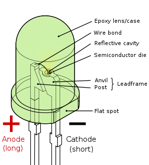
Parts of an LED

Efficiency and operational parameters
Typical indicator LEDs are designed to operate with no more than 30–60 milliwatts [mW] of electrical power. Around 1999, Philips Lumileds introduced power LEDs capable of continuous use at one watt [W]. These LEDs used much larger semiconductor die sizes to handle the large power inputs. Also, the semiconductor dies were mounted onto metal slugs to allow for heat removal from the LED die.
One of the key advantages of LED-based lighting is its high efficiency, as measured by its light output per unit power input. White LEDs quickly matched and overtook the efficiency of standard incandescent lighting systems. In 2002, Lumileds made five-watt LEDs available with a luminous efficacy of 18–22 lumens per watt [lm/W]. For comparison, a conventional 60–100 W incandescent lightbulb produces around 15 lm/W, and standard fluorescent lights produce up to 100 lm/W. A recurring problem is that efficiency will fall dramatically for increased current. This effect is known as droop and effectively limits the light output of a given LED, increasing heating more than light output for increased current.
In September 2003, a new type of blue LED was demonstrated by the company Cree, Inc. to provide 24 mW at 20 milliamperes [mA]. This produced a commercially packaged white light giving 65 lm/W at 20 mA, becoming the brightest white LED commercially available at the time, and more than four times as efficient as standard incandescents. In 2006 they demonstrated a prototype with a record white LED luminous efficacy of 131 lm/W at 20 mA. Also, Seoul Semiconductor has plans for 135 lm/W by 2007 and 145 lm/W by 2008, which would be approaching an order of magnitude improvement over standard incandescents and better even than standard fluorescents. Nichia Corporation has developed a white LED with luminous efficacy of 150 lm/W at a forward current of 20 mA.
High-power (≥ 1 W) LEDs are necessary for practical general lighting applications. Typical operating currents for these devices begin at 350 mA.
Note that these efficiencies are for the LED chip only, held at low temperature in a lab. In a lighting application, operating at higher temperature and with drive circuit losses, efficiencies are much lower. United States Department of Energy (DOE) testing of commercial LED lamps designed to replace incandescent lamps or CFLs showed that average efficacy was still about 46 lm/W in 2009 (tested performance ranged from 17 lm/W to 79 lm/W).
Cree issued a press release on February 3, 2010 about a laboratory prototype LED achieving 208 lumens per watt at room temperature. The correlated color temperature was reported to be 4579 K

The inner workings of an LED


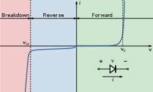
I-V diagram for a diode an LED will begin to emit light when the on-voltage is exceeded. Typical on voltages are 2-3 Volt

Lifetime and failure

Solid state devices such as LEDs are subject to very limited wear and tear if operated at low currents and at low temperatures. Many of the LEDs produced in the 1970s and 1980s are still in service today. Typical lifetimes quoted are 25,000 to 100,000 hours but heat and current settings can extend or shorten this time significantly.
The most common symptom of LED (and diode laser) failure is the gradual lowering of light output and loss of efficiency. Sudden failures, although rare, can occur as well. Early red LEDs were notable for their short lifetime. With the development of high-power LEDs the devices are subjected to higher junction temperatures and higher current densities than traditional devices. This causes stress on the material and may cause early light output degradation. To quantitatively classify lifetime in a standardized manner it has been suggested to use the terms L75 and L50 which is the time it will take a given LED to reach 75% and 50% light output respectively.
Like other lighting devices, LED performance is temperature dependent. Most manufacturers' published ratings of LEDs are for an operating temperature of 25°C. LEDs used outdoors, such as traffic signals or in-pavement signal lights, and that are utilized in climates where the temperature within the luminaire gets very hot, could result in low signal intensities or even failure.
LEDs maintain consistent light output even in cold temperatures, unlike traditional lighting methods. Consequently, LED technology may be a good replacement in areas such as supermarket freezer lighting and will last longer than other technologies. Because LEDs do not generate as much heat as incandescent bulbs, they are an energy-efficient technology to use in such applications such as freezers. On the other hand, because they do not generate much heat, ice and snow may build up on the LED luminaire in colder climates. This has been a problem plaguing airport runway lighting, although some research has been done to try to develop heat sink technologies in order to transfer heat to alternative areas of the luminaire.

Colors and materials

Color
Wavelength (nm)
Voltage (V)
Semiconductor Material
Infrared
λ > 760
ΔV < 1.9
Gallium arsenide (GaAs)
Aluminium gallium arsenide (AlGaAs)
Red
610 < λ < 760
1.63 < ΔV < 2.03
Aluminium gallium arsenide (AlGaAs)
Gallium arsenide phosphide (GaAsP)
Aluminium gallium indium phosphide (AlGaInP)
Gallium(III) phosphide (GaP)
Orange
590 < λ < 610
2.03 < ΔV < 2.10
Gallium arsenide phosphide (GaAsP)
Aluminium gallium indium phosphide (AlGaInP)
Gallium(III) phosphide (GaP)
Yellow
570 < λ < 590
2.10 < ΔV < 2.18
Gallium arsenide phosphide (GaAsP)
Aluminium gallium indium phosphide (AlGaInP)
Gallium(III) phosphide (GaP)
Green
500 < λ < 570
1.9 < ΔV < 4.0
Indium gallium nitride (InGaN) / Gallium(III) nitride (GaN)
Gallium(III) phosphide (GaP)
Aluminium gallium indium phosphide (AlGaInP)
Aluminium gallium phosphide (AlGaP)
Blue
450 < λ < 500
2.48 < ΔV < 3.7
Zinc selenide (ZnSe)
Indium gallium nitride (InGaN)
Silicon carbide (SiC) as substrate
Silicon (Si) as substrate — (under development)
Violet
400 < λ < 450
2.76 < ΔV < 4.0
Indium gallium nitride (InGaN)
Purple
multiple types
2.48 < ΔV < 3.7
Dual blue/red LEDs,
blue with red phosphor,
or white with purple plastic
Ultraviolet
λ < 400
3.1 < ΔV < 4.4
Diamond (235 nm)
Boron nitride (215 nm)
Aluminium nitride (AlN) (210 nm)
Aluminium gallium nitride (AlGaN)
Aluminium gallium indium nitride (AlGaInN)
 (down to 210 nm)
White
Broad spectrum
ΔV = 3.5
Blue/UV diode with yellow phosphor  


Types


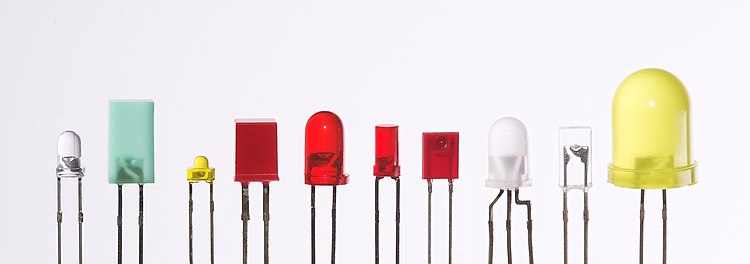
LEDs are produced in a variety of shapes and sizes. The 5 mm cylindrical package (red, fifth from the left) is the most common, estimated at 80% of world production. The color of the plastic lens is often the same as the actual color of light emitted, but not always. For instance, purple plastic is often used for infrared LEDs, and most blue devices have clear housings. There are also LEDs in SMT packages, such as those found on blinkies and on cell phone keypads (not shown).

Miniature LEDs

These are mostly single-die LEDs used as indicators, and they come in various-sizes from 2 mm to 8 mm, through-hole and surface mount packages. They are usually simple in design, not requiring any separate cooling body.[67] Typical current ratings ranges from around 1 mA to above 20 mA. The small scale sets a natural upper boundary on power consumption due to heat caused by the high current density and need for heat sinking.

Different sized LEDs. 8 mm, 5 mm and 3 mm, with a wooden match-stick for scale.

High power LEDs

High power LEDs (HPLED) can be driven at currents from hundreds of mA to more than an ampere, compared with the tens of mA for other LEDs. Some can produce over a thousand [68][69] lumens. Since overheating is destructive, the HPLEDs must be mounted on a heat sink to allow for heat dissipation. If the heat from a HPLED is not removed, the device will burn out in seconds. A single HPLED can often replace an incandescent bulb in a torch, or be set in an array to form a powerful LED lamp.
Some well-known HPLEDs in this category are the Lumileds Rebel Led, Osram Opto Semiconductors Golden Dragon and Cree X-lamp. As of September 2009 some HPLEDs manufactured by Cree Inc. now exceed 105 lm/W [70] (e.g. the XLamp XP-G LED chip emitting Cool White light) and are being sold in lamps intended to replace incandescent, halogen, and even fluorescent style lights as LEDs become more cost competitive.
LEDs have been developed by Seoul Semiconductor that can operate on AC power without the need for a DC converter. For each half cycle part of the LED emits light and part is dark, and this is reversed during the next half cycle. The efficacy of this type of HPLED is typically 40 lm/W.[71] A large number of LED elements in series may be able to operate directly from line voltage. In 2009 Seoul Semiconductor released a high DC voltage capable of being driven from AC power with a simple controlling circuit. The low power dissipation of these LEDs affords them more flexibility than the original AC LED design.

High-power light emiting diodes 

Mid-range LEDs

Medium power LEDs are often through-hole mounted and used when an output of a few lumen is needed. They sometimes have the diode mounted to four leads (two cathode leads, two anode leads) for better heat conduction and carry an integrated lens. An example of this is the Superflux package, from Philips Lumileds. These LEDs are most commonly used in light panels, emergency lighting and automotive tail-lights. Due to the larger amount of metal in the LED, they are able to handle higher currents (around 100 mA). The higher current allows for the higher light output required for tail-lights and emergency lighting.

Application-specific variations

Flashing LEDs are used as attention seeking indicators without requiring external electronics. Flashing LEDs resemble standard LEDs but they contain an integrated multivibrator circuit which causes the LED to flash with a typical period of one second. In diffused lens LEDs this is visible as a small black dot. Most flashing LEDs emit light of a single color, but more sophisticated devices can flash between multiple colors and even fade through a color sequence using RGB color mixing.
Bi-color LEDs are actually two different LEDs in one case. They consist of two dies connected to the same two leads antiparallel to each other. Current flow in one direction produces one color, and current in the opposite direction produces the other color. Alternating the two colors with sufficient frequency causes the appearance of a blended third color. For example, a red/green LED operated in this fashion will color blend to produce a yellow appearance.
Tri-color LEDs are two LEDs in one case, but the two LEDs are connected to separate leads so that the two LEDs can be controlled independently and lit simultaneously. A three-lead arrangement is typical with one common lead (anode or cathode).
RGB LEDs contain red, green and blue emitters, generally using a four-wire connection with one common lead (anode or cathode). These LEDs can have either common positive or common negative leads. Others however, have only two leads (positive and negative) and have a built in tiny electronic control unit.
Alphanumeric LED displays are available in seven-segment and starburst format. Seven-segment displays handle all numbers and a limited set of letters. Starburst displays can display all letters. Seven-segment LED displays were in widespread use in the 1970s and 1980s, but increasing use of liquid crystal displays, with their lower power consumption and greater display flexibility, has reduced the popularity of numeric and alphanumeric LED displays.

Considerations for use

Power sources

The current/voltage characteristic of an LED is similar to other diodes, in that the current is dependent exponentially on the voltage (see Shockley diode equation). This means that a small change in voltage can lead to a large change in current. If the maximum voltage rating is exceeded by a small amount the current rating may be exceeded by a large amount, potentially damaging or destroying the LED. The typical solution is therefore to use constant current power supplies, or driving the LED at a voltage much below the maximum rating. Since most household power sources (batteries, mains) are not constant current sources, most LED fixtures must include a power converter. However, the I/V curve of nitride-based LEDs is quite steep above the knee and gives an If of a few milliamperes at a Vf of 3 V, making it possible to power a nitride-based LED from a 3 V battery such as a coin cell without the need for a current limiting resistor.

Electrical polarity

As with all diodes, current flows easily from p-type to n-type material. However, no current flows and no light is produced if a small voltage is applied in the reverse direction. If the reverse voltage becomes large enough to exceed the breakdown voltage, a large current flows and the LED may be damaged. If the reverse current is sufficiently limited to avoid damage, the reverse-conducting LED is a useful noise diode.

Safety

The vast majority of devices containing LEDs are "safe under all conditions of normal use", and so are classified as "Class 1 LED product"/"LED Klasse 1". At present, only a few LEDs—extremely bright LEDs that also have a tightly focused viewing angle of 8° or less—could, in theory, cause temporary blindness, and so are classified as "Class 2". In general, laser safety regulations—and the "Class 1", "Class 2", etc. system—also apply to LEDs.

Advantages

-Efficiency: LEDs produce more light per watt than incandescent bulbs.[75] Their efficiency is not affected by shape and size, unlike Fluorescent light bulbs or tubes.
-Color: LEDs can emit light of an intended color without the use of the color filters that traditional lighting methods require. This is more efficient and can lower initial costs.
-Size: LEDs can be very small (smaller than 2 mm2) and are easily populated onto printed circuit boards.
-On/Off time: LEDs light up very quickly. A typical red indicator LED will achieve full brightness in under a microsecond. LEDs used in communications devices can have even faster response times.
-Cycling: LEDs are ideal for use in applications that are subject to frequent on-off cycling, unlike fluorescent lamps that burn out more quickly when cycled frequently, or HID lamps that require a long time before restarting.
-Dimming: LEDs can very easily be dimmed either by pulse-width modulation or lowering the forward current.
-Cool light: In contrast to most light sources, LEDs radiate very little heat in the form of IR that can cause damage to sensitive objects or fabrics. Wasted energy is dispersed as heat through the base of the LED.
-Slow failure: LEDs mostly fail by dimming over time, rather than the abrupt burn-out of incandescent bulbs.
-Lifetime: LEDs can have a relatively long useful life. One report estimates 35,000 to 50,000 hours of useful life, though time to complete failure may be longer. Fluorescent tubes typically are rated at about 10,000 to 15,000 hours, depending partly on the conditions of use, and incandescent light bulbs at 1,000–2,000 hours.
-Shock resistance: LEDs, being solid state components, are difficult to damage with external shock, unlike fluorescent and incandescent bulbs which are fragile.
-Focus: The solid package of the LED can be designed to focus its light. Incandescent and fluorescent sources often require an external reflector to collect light and direct it in a usable manner.
-Toxicity: LEDs do not contain mercury, unlike fluorescent lamps.

Disadvantages

-Some Fluorescent lamps can be more efficient.
-High initial price: LEDs are currently more expensive, price per lumen, on an initial capital cost basis, than most conventional lighting technologies. The additional expense partially stems from the relatively low lumen output and the drive circuitry and power supplies needed.
-Temperature dependence: LED performance largely depends on the ambient temperature of the operating environment. Over-driving the LED in high ambient temperatures may result in overheating of the LED package, eventually leading to device failure. Adequate heat-sinking is required to maintain long life. This is especially important when considering automotive, medical, and military applications where the device must operate over a large range of temperatures, and is required to have a low failure rate.
-Voltage sensitivity: LEDs must be supplied with the voltage above the threshold and a current below the rating. This can involve series resistors or current-regulated power supplies.
-Light quality: Most cool-white LEDs have spectra that differ significantly from a black body radiator like the sun or an incandescent light. The spike at 460 nm and dip at 500 nm can cause the color of objects to be perceived differently under cool-white LED illumination than sunlight or incandescent sources, due to metamerism, red surfaces being rendered particularly badly by typical phosphor based cool-white LEDs. However, the color rendering properties of common fluorescent lamps are often inferior to what is now available in state-of-art white LEDs.
-Area light source: LEDs do not approximate a "point source" of light, but rather a lambertian distribution. So LEDs are difficult to use in applications requiring a spherical light field. LEDs are not capable of providing divergence below a few degrees. This is contrasted with lasers, which can produce beams with divergences of 0.2 degrees or less.
-Blue hazard: There is a concern that blue LEDs and cool-white LEDs are now capable of exceeding safe limits of the so-called blue-light hazard as defined in eye safety specifications such as ANSI/IESNA RP-27.1-05: Recommended Practice for Photobiological Safety for Lamp and Lamp Systems.
-Blue pollution: Because cool-white LEDs, emit proportionally more blue light than conventional outdoor light sources such as high-pressure sodium lamps, the strong wavelength dependence of Rayleigh scattering means that cool-white LEDs can cause more light pollution than other light sources. The International Dark-Sky Association discourages the use of white light sources with correlated color temperature above 3,000 K.

Applications

-Application of LEDs fall into four major categories:
-Visual signal application where the light goes more or less directly from the LED to the human eye, to convey a message or meaning.
-Illumination where LED light is reflected from object to give visual response of these objects.
-Generate light for measuring and interacting with processes that do not involve the human visual system.
-Narrow band light sensors where the LED is operated in a reverse-bias mode and is responsive to incident light instead of emitting light.


Freddy Vallenilla, EES SECC 2